
Semiconductor parts and semiconductor mounting apparatus

a technology of semiconductor and semiconductor parts, applied in the direction of optical elements, coupling device connections, instruments, etc., can solve the problems of increased heat generation, crosstalk between wiring, increased wiring resistance, etc., and achieve the effect of accurate registry

Inactive Publication Date: 2002-02-28
FUJITSU LTD
View PDF0 Cites 8 Cited by
  • Summary
  • Abstract
  • Description
  • Claims
  • Application Information

AI Technical Summary

Benefits of technology

[0019] In order to solve the above-mentioned problem, according to the invention, a socket for receiving a semiconductor part including photoelectric elements is arranged on a printed board. According to claim 1, the position of packaging a semiconductor part on the printed board is defined, and therefore the accuracy of registry between the optical transmission path on the printed board and the optical device of the semiconductor part is improved.
[0021] Preferably, the semiconductor part inserted into the socket and the insertion holes of the socket for the semiconductor part are placed in spaced relation to each other. As a result, the correct position of arrangement of the semiconductor part is held within a predefined range, resulting in an improved working efficiency.
[0030] Preferably, there is provided a printed board on which a semiconductor part including light-emitting elements, photo-detectors and photoelectric elements is packaged. Further, an optical transmission path with an end thereof optically coupled to the light-emitting elements of the semiconductor part and with the other end thereof optically coupled to the photo-detectors is arranged on the printed board. The board has such a structure that the optical signal transmitted from the semiconductor part is returned to the semiconductor part through the optical transmission path arranged on the printed board. Superior optical coupling is achieved between two points of the printed board and two points of the semiconductor part, thereby guaranteeing the arrangement of the semiconductor elements at the correct position.
[0032] Preferably, there is provided a printed board unit in which a semiconductor part including an optical device is fixed by an adhesive on the board. The semiconductor part is fixed on the printed board without stress, and therefore the durability is improved.
[0034] Preferably, the positioning apparatus includes a power terminal for supplying power to the optical device of the semiconductor part. A part dedicated to registration need not be arranged on the printed board, and a reduction in density of the wiring and the parts on the printed board can be prevented.
[0036] Preferably, the semiconductor part including an optical device is fixed on the printed board using an adhesive. In other words, the soldering is eliminated, thereby solving the problem that the semiconductor part is broken by the high-temperature heat generated by the soldering process.

Problems solved by technology

With an increase in signal transmission speed and an increased density of wirings and parts, the technique of electrically interconnecting parts on a printed board has posed the problem that an increased wiring resistance, due to the skin effect, appears and that crosstalk between wiring is caused during communication between the parts.
The increased wiring resistance leads to an increased heat generation and the crosstalk disturbs the signal waveform causing a malfunction.
In this way, electrical methods of interconnection have almost come to a limit of speed and density.
Also, the LD (laser diode) used as the light-emitting element and the PD (photo-diode) used as the photo-detector have a low heat resistance, and are liable to be broken by a thermal stress when soldered for packaging.
Unless both the light-emitting elements and the photo-detectors of the semiconductor part are optically coupled to the openings of the optical transmission path, the semiconductor elements cannot receive the optical signal emitted by themselves.
Unless the photoelectric elements of the semiconductor part are optically coupled to both the inlet and outlet of the optical transmission path, however, the optical transmission path can neither receive nor output the optical signal.

Method used


Image

  • Semiconductor parts and semiconductor mounting apparatus
  • Semiconductor parts and semiconductor mounting apparatus
  • Semiconductor parts and semiconductor mounting apparatus

Examples


Embodiment Construction

[0058] Embodiments of the present invention will be explained below.

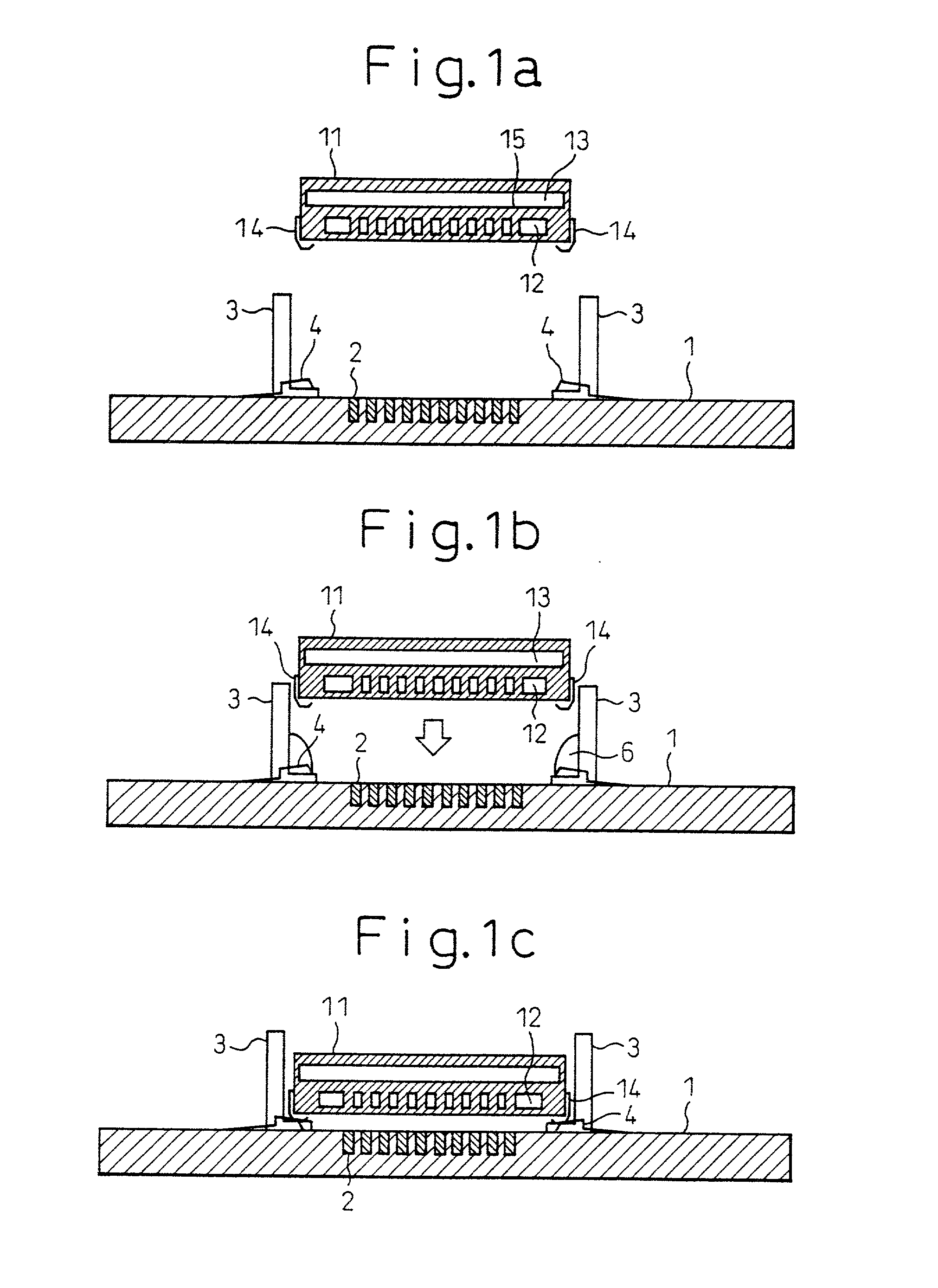
[0059] FIGS. 1a to 1c are diagrams showing the process of mounting an OEIC package on a printed board. Sectional views of the printed board and the OEIC package mounted on the printed board are shown in each drawing.

[0060] In FIGS. 1a to 1c, 1 designates a printed board, 2 waveguides, 3 a connector socket, 4 power terminals or ground terminals, 6 an adhesive, 11 an OEIC package, 12 an optical device array, 13 an electrical circuit chip and 14 a package-side power terminal or ground terminal.

[0061] FIG. 1a shows the first step of mounting.

[0062] The OEIC package 11 has sealed therein the optical device array 12 and the electrical circuit chip 13, which are electrically connected to each other through ball bumps 15. The optical device array 12 has arranged thereon LDs (laser diodes) as light-emitting elements and PDs (photo-diodes) as photo-detectors. The electrical signal output from the electrical circuit chip 13 is...


PUM

PropertyMeasurementUnit
diameteraaaaaaaaaa
diameteraaaaaaaaaa
diameteraaaaaaaaaa

Abstract

To provide a package structure for securing a satisfactory optical coupling between an optical device arranged beforehand on a printed board and an optical device newly mounted on the particular printed board. Positioning LDs 41a and 41b are arranged on a printed board 1. A sensing PD 42a for receiving the optical signal emitted from the positioning LD 41a and a sensing PD 42b for receiving the optical signal emitted from the positioning LD 41b are arranged in an OEIC package 11 mounted on the printed board.

Description

[0001] 1. Field of the Invention[0002] The present invention relates to a structure for interconnection between semiconductor chips, between MCMs (multichip modules) or between an MCM and a semiconductor chip packaged on a printed board, or more in particular to a structure for mounting a semiconductor or an MCM accurately at a predetermined position on the board in order to obtain a superior optical coupling between the parts and an optical waveguide for optical communication between the parts on the printed board.[0003] 2. Description of the Related Art[0004] With an increase in signal transmission speed and an increased density of wirings and parts, the technique of electrically interconnecting parts on a printed board has posed the problem that an increased wiring resistance, due to the skin effect, appears and that crosstalk between wiring is caused during communication between the parts. The increased wiring resistance leads to an increased heat generation and the crosstalk di...

Claims


Application Information

Patent Timeline
Patent Type & Authority Applications(United States)
IPC IPC(8): H01R33/76G02B6/42H01L23/32H05K1/02H05K3/30H05K13/04
CPCG02B6/4224G02B6/4225G02B6/4227G02B6/4239G02B6/4249H01L2924/0002H05K1/0274H01L2924/00
Inventor WATANABE, TAKAYUKI
Owner FUJITSU LTD
Learn More