Microvia inspection system

a micro-organism and inspection system technology, applied in the field of micro-organism inspection systems, can solve problems such as inability to accurately inspect the structure of the microorganism, incorrect handling of the circuit board, and the board panel is often too expensive to scrap, and achieves the effect of higher resolution

Inactive Publication Date: 2002-03-07
AGILENT TECH INC
View PDF0 Cites 13 Cited by
  • Summary
  • Abstract
  • Description
  • Claims
  • Application Information

AI Technical Summary

Benefits of technology

0033] In one embodiment, the camera for capturing images from top lighting

Problems solved by technology

While these technologies are quite effective, in full-scale production various defects may arise due to problems such incorrect setting of drilling equipment, loading of incorrect files, incorrect handling of the circuit board, of residual debris in or near the microvia.
When defects arise the board panels are often too expensive to scrap and expensive re-work is required.
Existing inspecti

Method used


Image

  • Microvia inspection system
  • Microvia inspection system
  • Microvia inspection system

Examples


Embodiment Construction

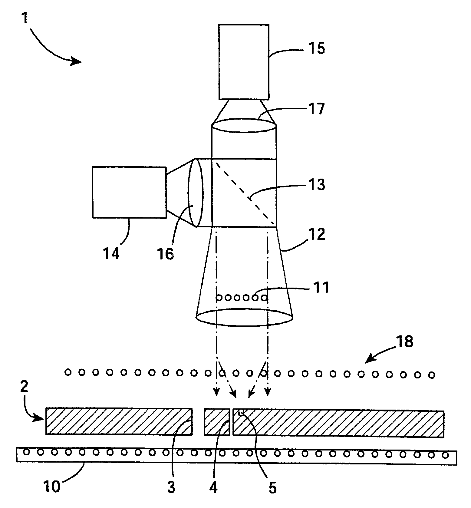
[0043] Referring to FIG. 1, a microvia inspection system 1 of the invention is shown. The system 1 is illustrated inspecting a circuit board 2 having a wide mechanically-drilled through via 3, a laser-drilled through microvia 4 and a laser-drilled blind microvia 5. The system is particularly suitable for detection of defects in through and blind microvias having a diameter in the range of 20 .mu.m to 200 .mu.m and a high aspect ratio (length over diameter).

[0044] The system 1 comprises a back lighting unit 10 comprising an array of 6000 LEDs of red colour and having an overall power output of 1-5 mW / LED. In general, there should be greater than 4000 LEDs. The back lighting unit 10 comprises a controller for switching sections of LEDs on a configurable basis so that the illumination corresponds to the board panel currently being inspected. The overall workspace illuminated by the back lighting unit 10 is 600 mm.times.450 mm.

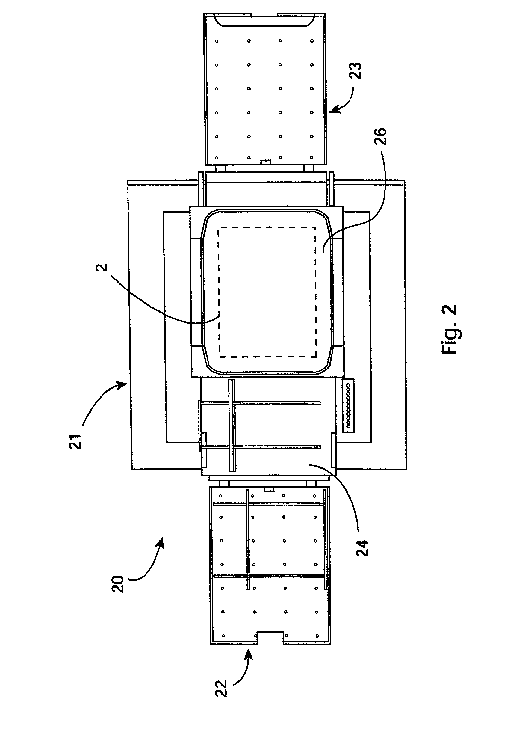
[0045] The unit 10 is mounted on a board conveying and suppo...


PUM


Abstract

A system (1) has a projection lens (12) directing on-axis light and low level LEDs (18) directing light to blind microvias (5). A high resolution camera (14) captures blind microvia images and an image processor recognizes defects according to classifications (54-59) according to reflected light area and centroid position. The lens (12) is telecentric for particularly effective image capture in blind microvias (5). The system also has an array of 6000 back lighting LEDs (10) providing illumination for capture of images by a camera (15). These images are analyzed by the image processor to detect defects such as blocked through microvias.

Description

[0001] The invention relates to inspection of microvias in circuit boards.PRIOR ART DISCUSSION[0002] In recent years there has been a very rapid move towards increased miniaturisation of circuits because of demands of industries such as the mobile telecommunications industry. Where multi-layer circuit boards are used there id frequent use of "blind" vias which do not extend fully through the board but instead penetrate part of the depth of the board to reach an internal layer to make an electrical connection. Whether the board is multi-layered or not, there is also frequent use of through vias to make connections from the front surface to the back surface.[0003] With increased miniaturisation and higher circuit densities, the sizes of the vias has been decreasing and they are now generally referred to as "microvias". Typically, the sizes range between 20 .mu.m and 75 .mu.m. The technologies to drill microvias involve use of high-precision laser beams. The laser may be of the CO2 or ...

Claims


Application Information

Patent Timeline
IPC IPC(8): G01N21/956G01R31/28G01R31/309G06T7/00H05K3/00
CPCG01N21/95692G01R31/2805G01R31/309G06T7/0006G06T2207/10152G06T2207/30141
Inventor OWEN, MARK DOUGLASBOYLE, ADRIANDORR, NIALLMAHON, JAMESCONLON, PETER
Owner AGILENT TECH INC
Why Eureka
Try Eureka