Electronic circuit device and hybrid integrated circuit with an asic and an FPGA

Inactive Publication Date: 2002-06-06
KK TOSHIBA
View PDF0 Cites 74 Cited by
  • Summary
  • Abstract
  • Description
  • Claims
  • Application Information

AI Technical Summary

Problems solved by technology

Unlike gate arrays, however, the complexity of standard cells can range from simple logic gates such as those found in gate arrays to block-level components such as RAMs, ROMs, PLAs and Maga-cells such as CPU cores.
Generally speaking, the packing density of ASIC is high to accommodate high performance hardware macrocells resulting in a higher cost performance

Method used


Image

  • Electronic circuit device and hybrid integrated circuit with an asic and an FPGA
  • Electronic circuit device and hybrid integrated circuit with an asic and an FPGA
  • Electronic circuit device and hybrid integrated circuit with an asic and an FPGA

Examples


Embodiment Construction

[0025] Several embodiments of the present invention will be described with reference to the accompanying drawings.

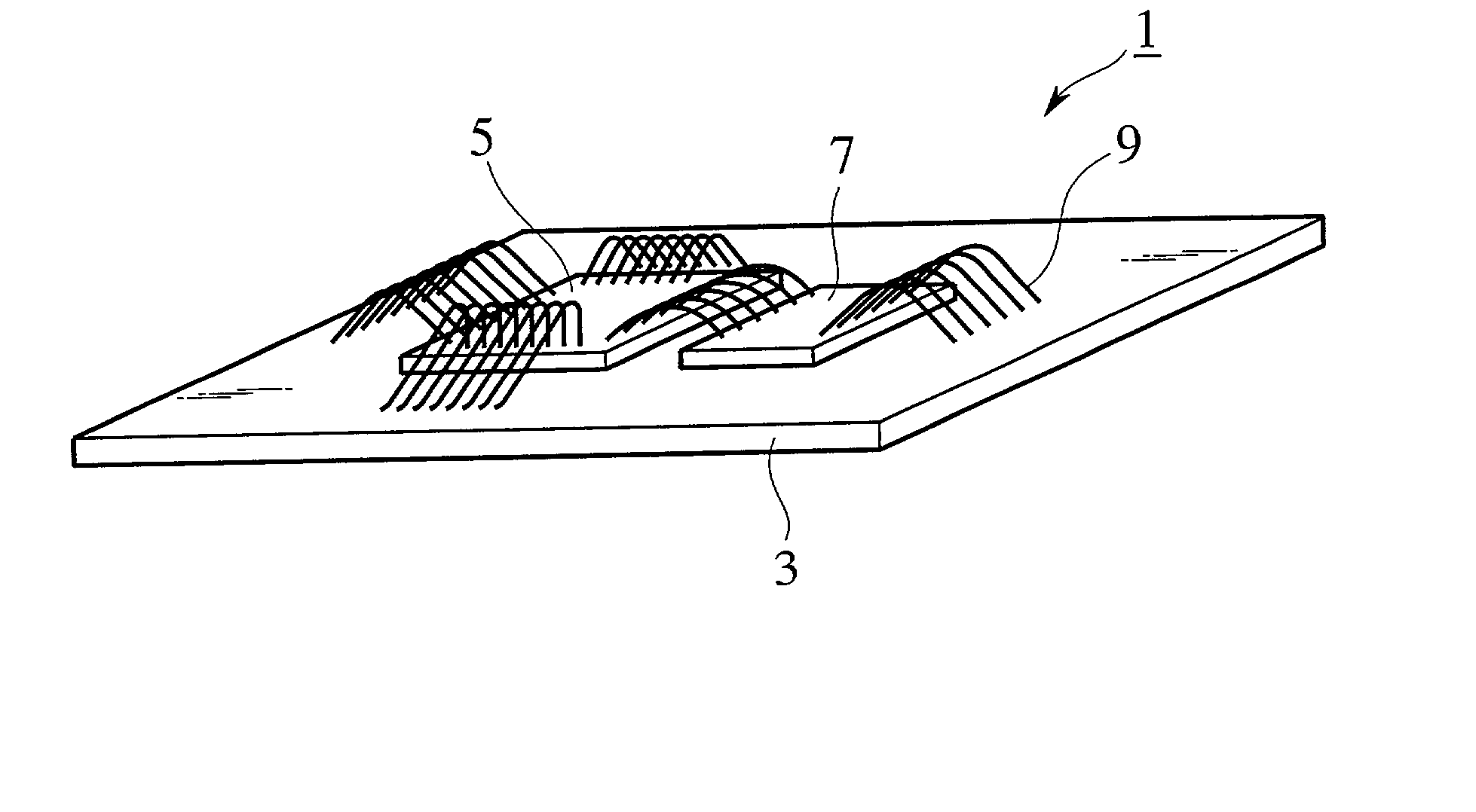
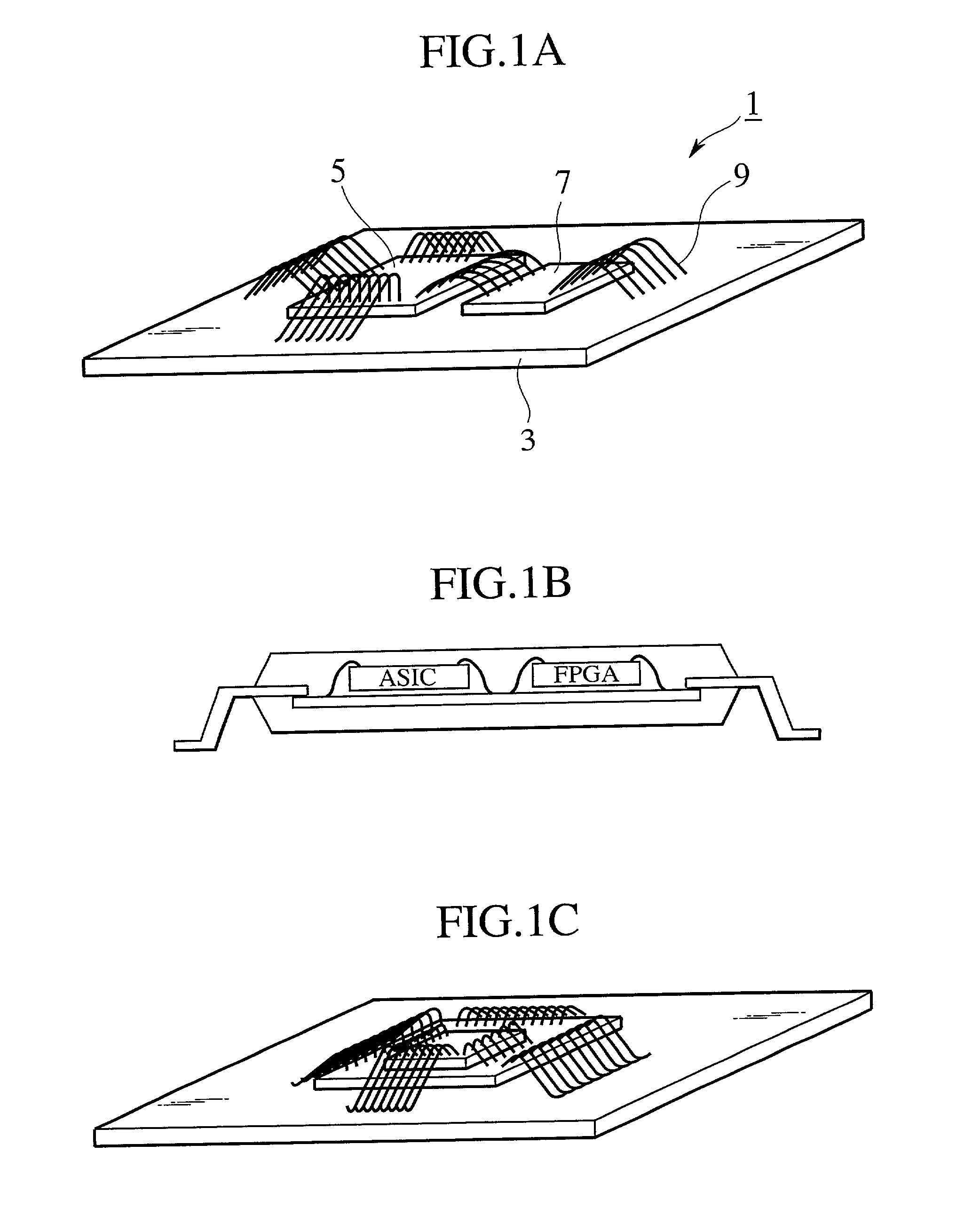
[0026] FIG. 1A and FIG. 1B are a cross sectional view and a perspective view showing a hybrid integrated circuit in accordance with an embodiment of the present invention. In this case, the hybrid integrated circuit 1 is composed of a ceramic substrate or a printed circuit board 3 as a common substrate in which are formed electrode patterns such as electrode pads for bonding, wiring patterns and so forth, a monolithic semiconductor integrated circuit 5 of an ASIC mounted on the ceramic substrate 3, another monolithic semiconductor integrated circuit 7 of an FPGA also mounted on the ceramic substrate 3 and gold wires 9 with which the monolithic semiconductor integrated circuits 5 and 7 and the ceramic substrate 3 are interconnected. These monolithic semiconductor integrated circuits 5 and 7 have been diced as semiconductor chips from a semiconductor wafer.

[0027] The monol...


PUM


Abstract

An improved hybrid integrated circuit is provided in order that the specification can quickly be modified and adjusted when required without need for preparing a new mask and without need for compromising the performance of the hybrid integrated circuit. The hybrid integrated circuit comprises: a common substrate on which an electrode pattern is formed; a first monolithic semiconductor chip designed by the use of an ASIC technology and mounted on the common substrate; a second monolithic semiconductor chip designed by the use of an FPGA technology and mounted on the common substrate; and external terminals provided for the common substrate; and an insulating material encapsulating the first monolithic semiconductor chip and the second monolithic semiconductor chip, wherein the second monolithic semiconductor chip is provided with a storage element which is rewritable by means of a control signal given through the external terminal in order to store circuit configuration data with which internal connections of the second monolithic semiconductor chip are modified to form a hardware configuration within the second monolithic semiconductor chip corresponding to a predetermined operational specification, and wherein the first monolithic semiconductor chip and the second monolithic semiconductor chip cooperate with each other by exchanging signals through the electrode pattern of the common substrate in order to implement the predetermined operational specification.

Description

[0001] This application is based upon and claims the benefit of priority from prior Japanese Patent Application P2000-367585 filed on Dec. 1, 2000; the entire contents of which are incorporated by reference herein.BACKGROUN OF THE INVENTION[0002] 1. Field of the Invention[0003] The present invention relates to a hybrid integrated circuit with an ASIC and an FPGA and an electronic circuit device.[0004] 2. Description of the Related Art[0005] In the recent years, the semiconductor integrated circuits have been broadly utilized which are called ASICs (Application Specific Circuits) in contrast with general purpose LSIs (Large Scale Integrated Circuits). Conventionally, there are two primary approaches, as employed for the purpose of reducing the development time, to developing integrated circuits called ASICs, i.e., the use of gate arrays and the use of standard cells.[0006] Gate arrays are integrated circuits having a fixed number of identical sites arranged in a regular manner, each ...

Claims


Application Information

Patent Timeline
IPC IPC(8): H01L25/18
CPCH01L25/18H01L2224/48137H01L2224/48225H01L2225/06568H01L2924/15311H01L2224/48227H01L2224/45144H01L2224/73265H01L2224/32145H01L2224/32225H01L2224/48145H01L2924/00012H01L2924/00H01L24/73H01L2924/14
Inventor TAGUCHI, HIDEKI
Owner KK TOSHIBA
Why Eureka
Try Eureka