Passivation scheme for bumped wafers

a technology of bumped wafers and passivation schemes, which is applied in the direction of semiconductor devices, electrical equipment, semiconductor/solid-state device details, etc., can solve the problems of increased processing expanse, extra steps, and expensive planarization process in wafer manufactur

Inactive Publication Date: 2002-06-06
SEMICON COMPONENTS IND LLC
View PDF2 Cites 66 Cited by
  • Summary
  • Abstract
  • Description
  • Claims
  • Application Information

AI Technical Summary

Problems solved by technology

The passivation process for today's wafers generally include masking steps and an expensive planarization process.
However, as noted, such use can result in extra steps and increased processing expanse in wafer manufacture.

Method used


Image

  • Passivation scheme for bumped wafers
  • Passivation scheme for bumped wafers
  • Passivation scheme for bumped wafers

Examples


Embodiment Construction

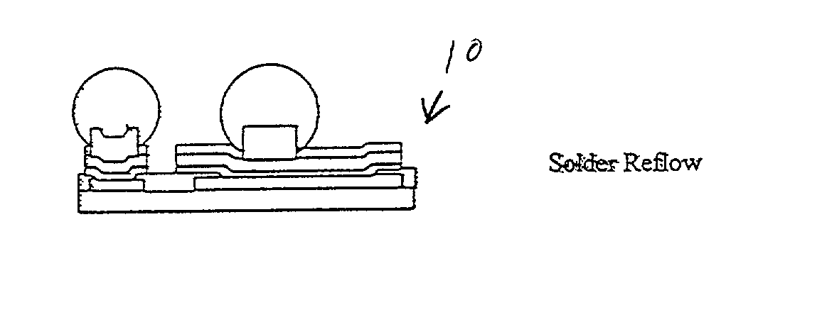
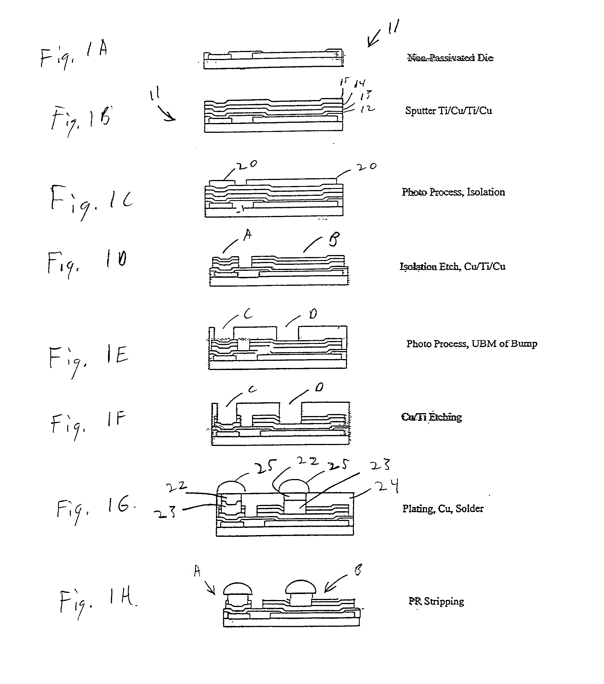
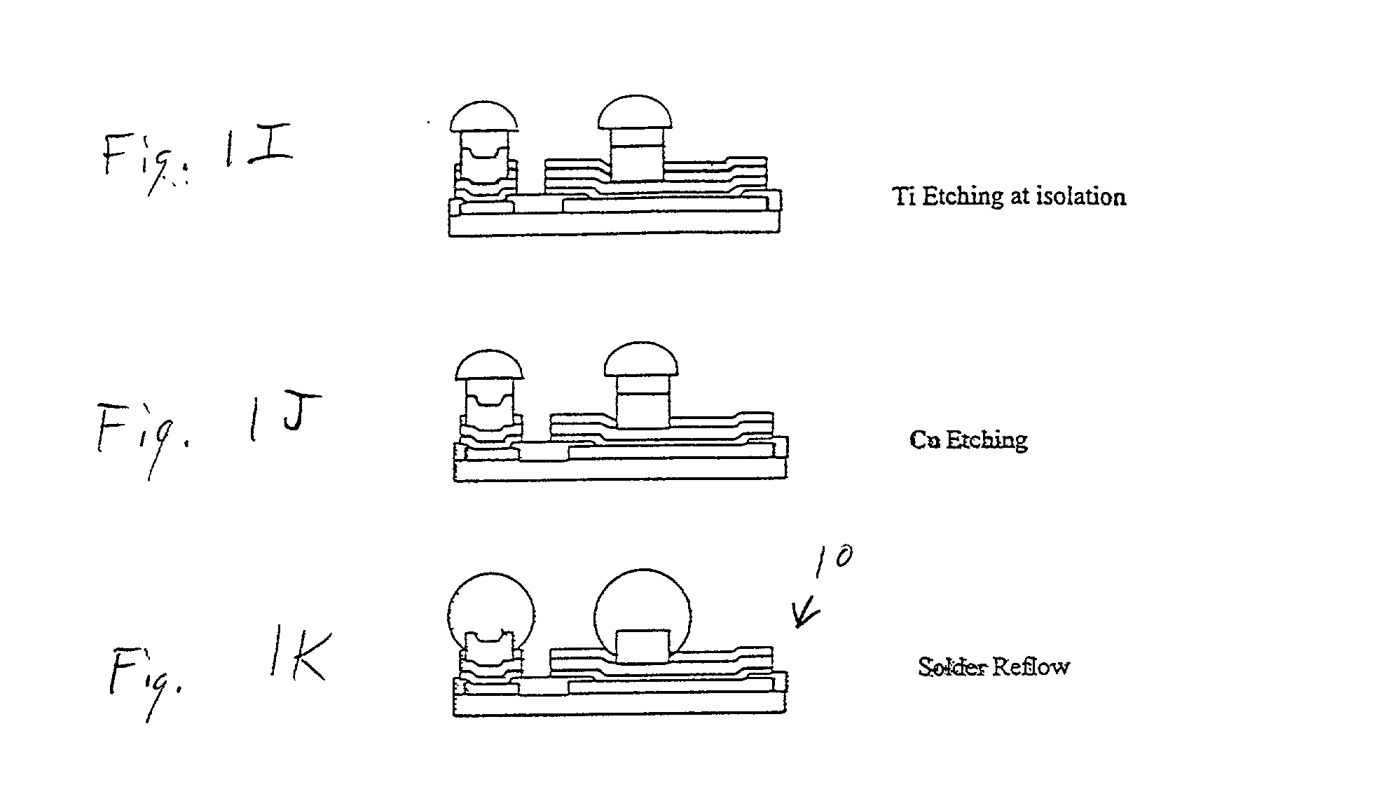
[0011] FIG. 1K schematically illustrates a bumped wafer 10 in accordance with the present invention. The bumped wafer includes a non-passivated die and various layers of material deposited thereon. Additionally, the bumped wafer includes solder bumps.

[0012] Turning to FIG. 1A, a non-passivated die 11 is illustrated. FIG. 1B illustrates the non-passivated die with a first layer of titanium 12 sputtered thereon, a first layer of copper 13 sputtered on the first layer of titanium, a second layer of titanium 14 sputtered on the first layer of copper, and a second layer of copper 15 sputtered on the second layer of titanium.

[0013] Turning to FIG. 1C, a photo resist material 20 is placed over the second layer of copper for isolation purposes. FIG. 1D illustrates the etching away of the photo resist layer along with the second layer of copper, the second layer of titanium and the first layer of copper between region A and region B that are to be isolated. Photo resist material 21 is then p...


PUM


Abstract

A bumped wafer for use in making a chip device. The bumped wafer includes two titanium layers sputtered alternatingly with two copper layers over a non-passivated die. The bumped wafer further includes under bump material under solder bumps contained thereon.

Description

[0001] 1. Field of the Invention[0002] The present invention relates to bumped wafers for chip devices, and more particularly, to a new passivation scheme for bumped wafers.[0003] 2. Description of the Prior Art[0004] The primary component of today's chip devices is at least one die. The die generally consists of a wafer that has been passivated. The passivation process for today's wafers generally include masking steps and an expensive planarization process.[0005] Because of the masking layers, the metal layer(s) is generally thinner. In a MOSFET device, a passivation layer is placed over the metal layer to protect it. This can result in an increased resistance from the drain to the source region when the chip device is on. Conventional passivation methods include using silicon nitride as a passivation layer. However, as noted, such use can result in extra steps and increased processing expanse in wafer manufacture.[0006] The present invention provides a bumped wafer that includes ...

Claims


Application Information

Patent Timeline
Patent Type & Authority Applications(United States)
IPC IPC(8): H01L21/60H01L23/485
CPCH01L24/11H01L2224/13099H01L2924/0001H01L2224/131H01L2924/13091H01L2924/01013H01L2924/01022H01L2924/01029H01L24/13H01L2924/01005H01L2924/01006H01L2924/01033H01L2924/014H01L24/03H01L24/05H01L24/14H01L2224/03831H01L2224/05001H01L2224/05022H01L2224/05027H01L2224/0508H01L2224/05572H01L2224/1147H01L2224/1403H01L2224/05647H01L2924/00014H01L2224/05124H01L2224/05147H01L2224/05166
Inventor JOSHI, RAJEEV
Owner SEMICON COMPONENTS IND LLC
Why Eureka
Try Eureka