Multiple input phase lock loop with hitless reference switching

a reference switching and input phase lock technology, applied in the field of digital timing circuits, can solve the problems of reducing the maximum size of the phase excursion, affecting the operation of the output clock, and generating phase perturbations on the output clock

Inactive Publication Date: 2002-06-13
ZARLINK SEMICON LTD
View PDF1 Cites 21 Cited by
  • Summary
  • Abstract
  • Description
  • Claims
  • Application Information

AI Technical Summary

Problems solved by technology

These specifications impose stringent requirements on the transfer characteristics between the input references and the generated output clocks, and in particular they specify limitations on phase perturbations that may be generated on output clocks as a result of switching between input references.
The fundamental disadvantage of this a

Method used


Image

  • Multiple input phase lock loop with hitless reference switching
  • Multiple input phase lock loop with hitless reference switching
  • Multiple input phase lock loop with hitless reference switching

Examples


Embodiment Construction

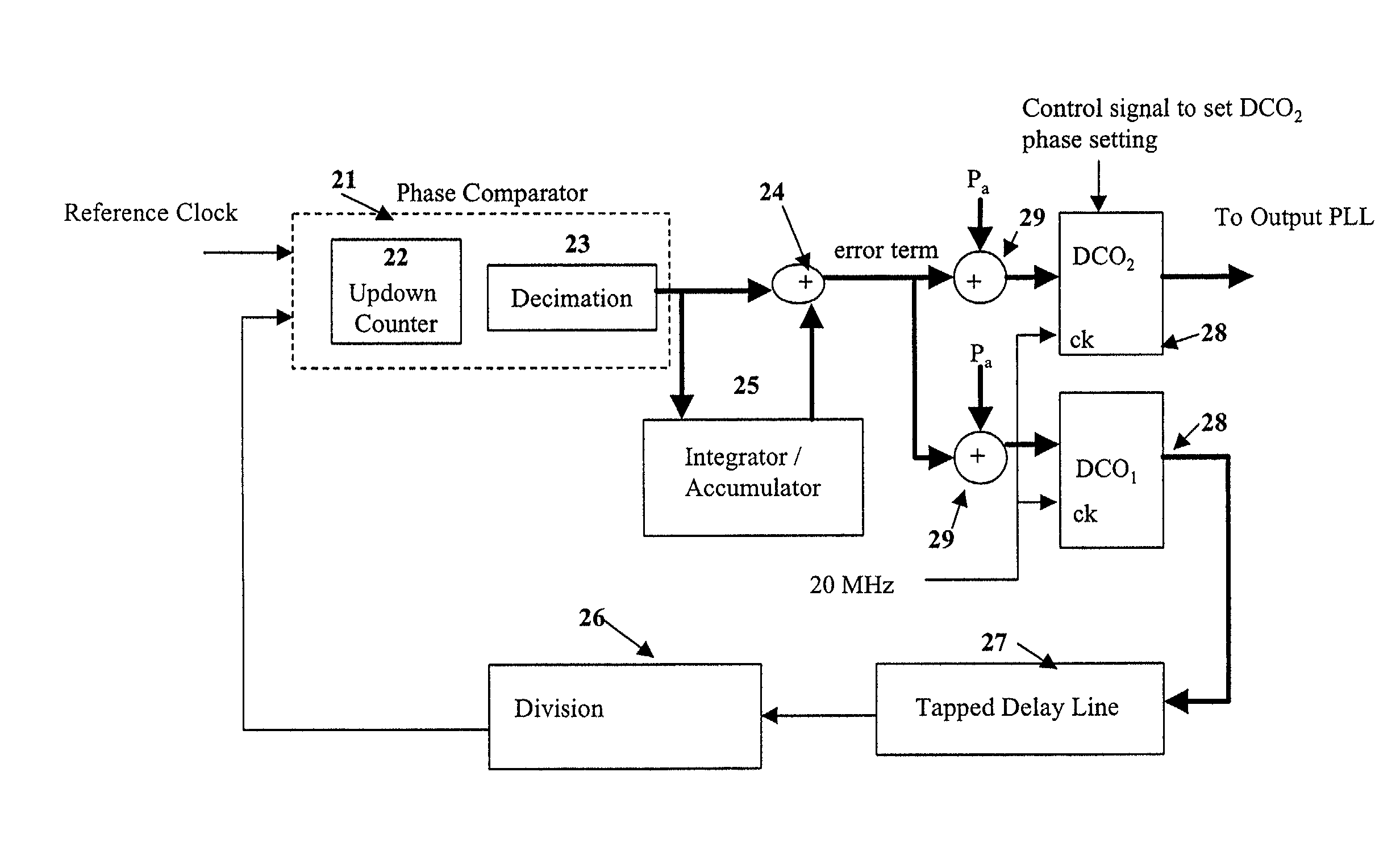
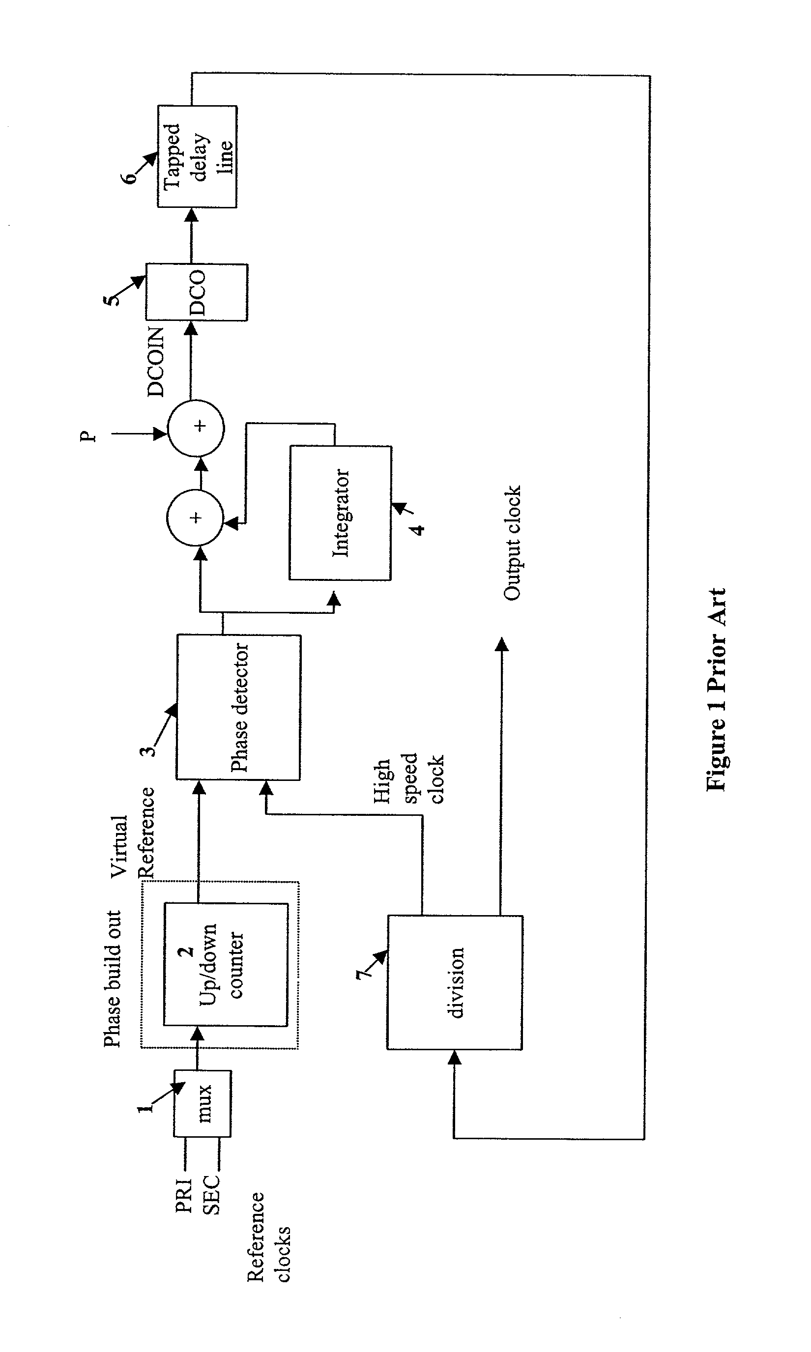
[0021] The prior art phase locked loop shown in FIG. 1 comprises a mux 1 selecting between two possible input reference clocks "pri" and "sec", a counter 2 that calibrates and builds out the phase difference between the two clocks upon reference switching, a phase detector 3 receiving a reference signal in, an integrator 4, a digital controlled oscillator 5 for generating an output signal at a desired frequency and a control signal representing the time error in the output signal, a tapped delay line 6 for receiving the output signal of the digital controlled oscillator 5, the tapped delay line 6 producing an output signal from a tap determined by said control signal, and a divider circuit 7 generating a feed back signal for the second input of the phase detector 3 and a synchronous high speed clock to the phase build out counter 2. The function of the integrator 4 is to eliminate input to output phase variations that would otherwise occur due to differences in the reference clock c...


PUM


Abstract

A clock recovery circuit for recovering clock signals from one of a plurality of input reference signals, includes an acquisition phase locked loop (PLL) for each input. The acquisition PLL having phase comparator for comparing the phase of an input signal to a feedback signal, and first and second digital controlled oscillators (DCOs) receiving an input from the phase comparator. The first DCO of the acquisition PLL is in a feedback loop to supply an input to the phase comparator and the second DCO of the acquisition PLL has a control input to introduce a phase offset therein relative to said the DCO of the acquisition PLL and provides an output for the acquisition PLL. An output PLL has a phase comparator selectively connectable to the output of each of the acquisition PLLs. The output PLL has a first DCO providing an output for the circuit and a second DCO in a feedback loop providing a feedback signal to the phase comparator of the output PLL. The second DCO of the output PLL has a control input to introduce a phase offset therein relative to the first DCO of the output PLL. A control unit for sets the phase of the second DCO of the acquisition circuit and the second DCO of the output PLL to a common value during changeover from one input to another to avoid an instantaneous phase error upon switching reference signals.

Description

[0001] 1. Field of the Invention[0002] This invention relates in general to digital timing circuits, and more particularly to a digital phase locked loop capable of recovering a clock signal from a choice of inputs signals subject to jitter.[0003] 2. Description of Related Art[0004] In digital networking applications, there is a requirement to provide timing reference for the SONET (synchronous optical network) OC-N and STS-N interface circuits, and TI or El primary rate digital transmission links. These timing signals must meet relevant standards such as BELLCORE GR-1244-CORE and GR-253-CORE recommendations for STRATUM 3E, 3 and 4E clocks and SONET Minimum Clock (SMC). These specifications impose stringent requirements on the transfer characteristics between the input references and the generated output clocks, and in particular they specify limitations on phase perturbations that may be generated on output clocks as a result of switching between input references.[0005] The method ...

Claims


Application Information

Patent Timeline
IPC IPC(8): H03L7/06H03L7/07H03L7/08H03L7/081H03L7/099H04J3/06
CPCH03L7/07H03L7/0805H04J3/0688H03L7/0994H03L7/081
Inventor SKIERSZKAN, SIMON
Owner ZARLINK SEMICON LTD
Why Eureka
Try Eureka