Thin film transistor for supplying power to element to be driven

Inactive Publication Date: 2002-06-20
SANYO ELECTRIC CO LTD
View PDF10 Cites 17 Cited by
  • Summary
  • Abstract
  • Description
  • Claims
  • Application Information

AI Technical Summary

Benefits of technology

0025] The switching thin film transistor is placed near the section where the selection line for selecting the transistor and the data line for supplying a data signal cross each other. In many cases, the switching thin film transistor is placed so that its channel length direction is approximately parallel to the extension direction of the selection line. In such a case, by placing the element driving thin film transistor so that its channel length direction is different from that of the switching thin film transistor, the channel length of the element driving thin film transistor can easily be increased.
0026] According to another aspect of the present invention, it is preferable that the element to be driven is an organic electrolumin

Problems solved by technology

Because of various reasons such as, for example, energy variation in the irradiating laser at the irradiation surface, the grain size of the polycrystalline silicon is not

Method used


Image

  • Thin film transistor for supplying power to element to be driven
  • Thin film transistor for supplying power to element to be driven
  • Thin film transistor for supplying power to element to be driven

Examples


first embodiment

[0048] First Embodiment

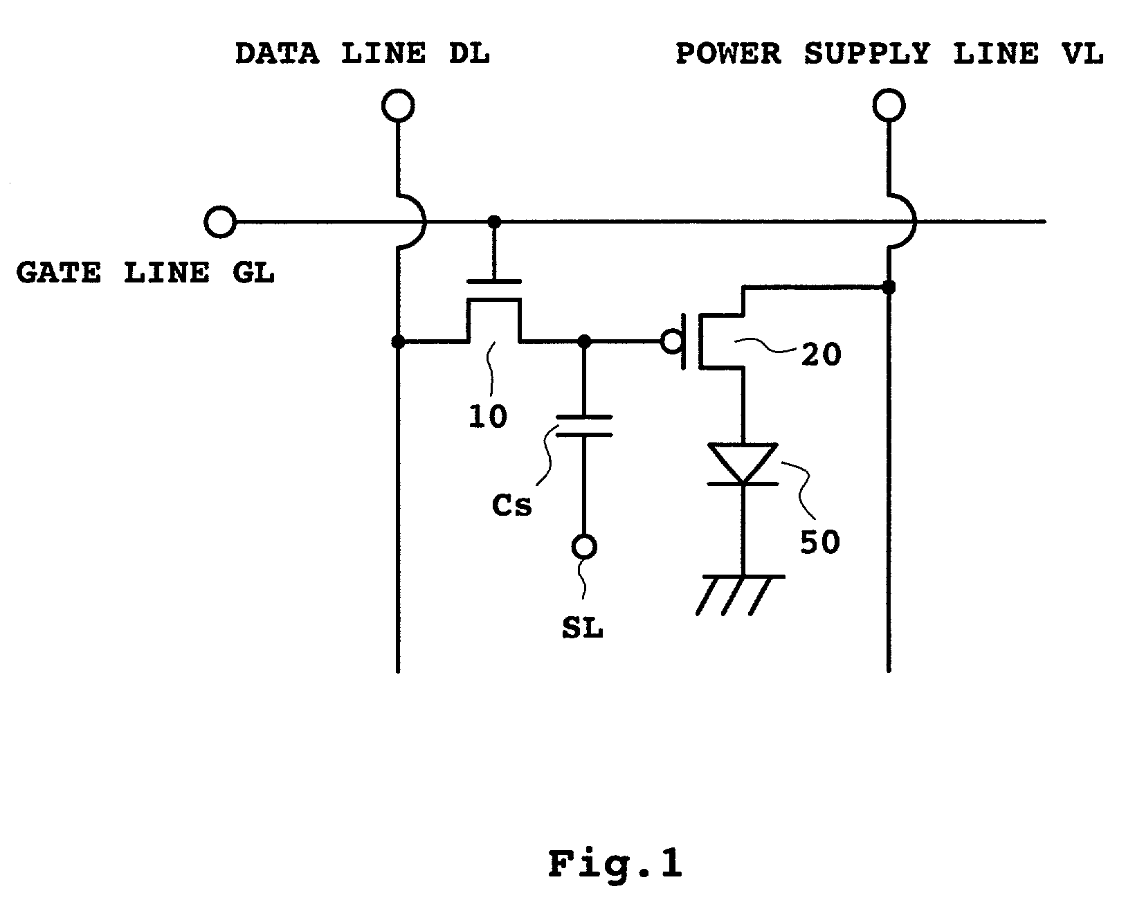
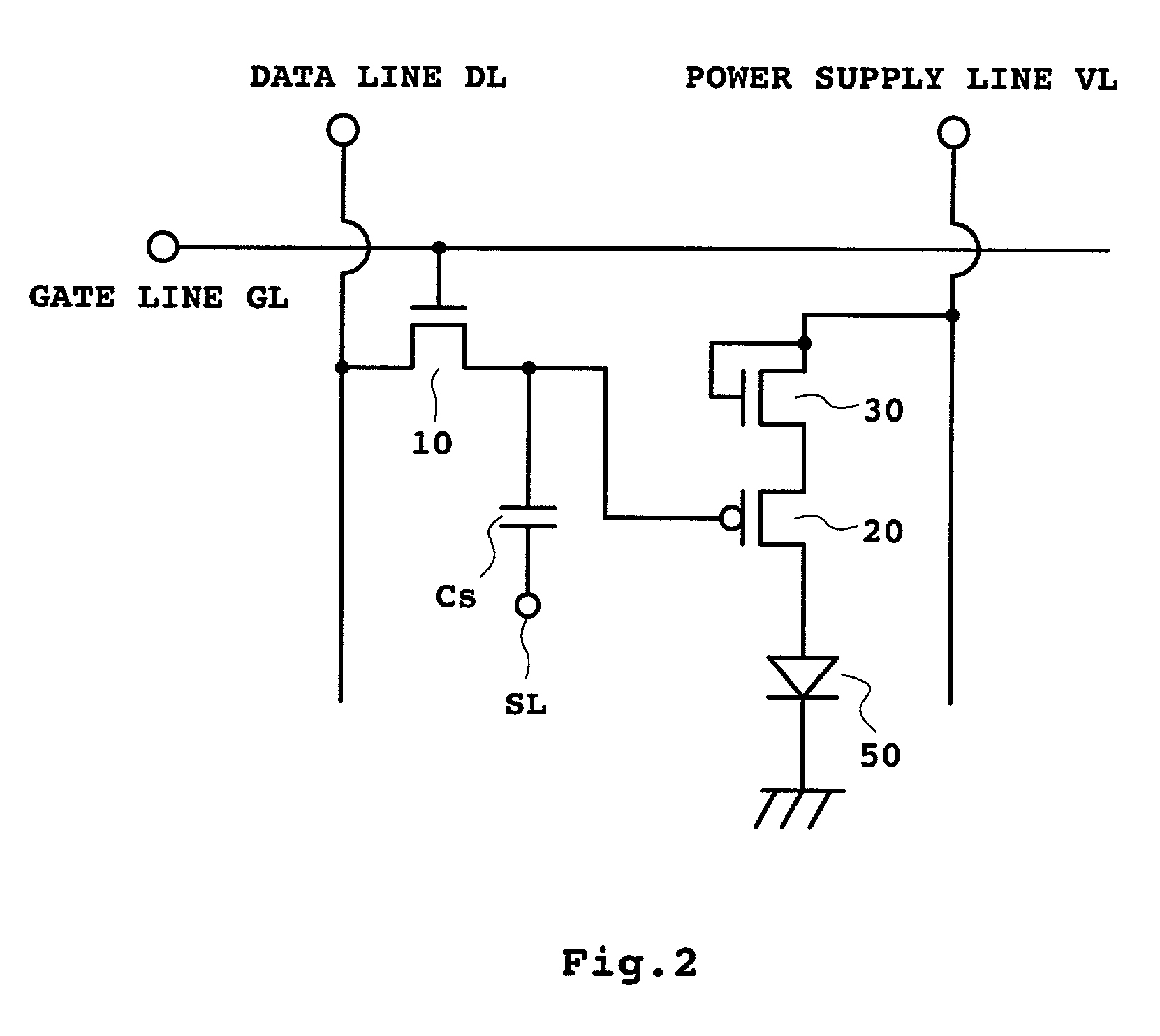
[0049] FIG. 2 shows a circuit structure of one pixel in an active matrix type EL display device having m rows and n columns according to a first embodiment of the present invention. As shown in FIG. 2, each pixel comprises an organic EL element 50, a switching TFT (first TFT) 10, an element driving TFT (second TFT) 20, and an storage capacitor Cs, and is constructed in a region surrounded by a gate line GL extending in the row direction and a data line DL extending in the column direction. In the first embodiment, a compensation TFT 30 having the conductive characteristic opposite of that of the second TFT 20 is provided between the power supply line VL and the second TFT 20. The gate and either the source or the drain of the compensation TFT 30 are connected to provide a diode connection. The diode is connected in the forward direction between the power supply line VL and the second TFT 20. Thus, the compensation TFT can be operated without supplying any desi...

second embodiment

[0084] Second Embodiment

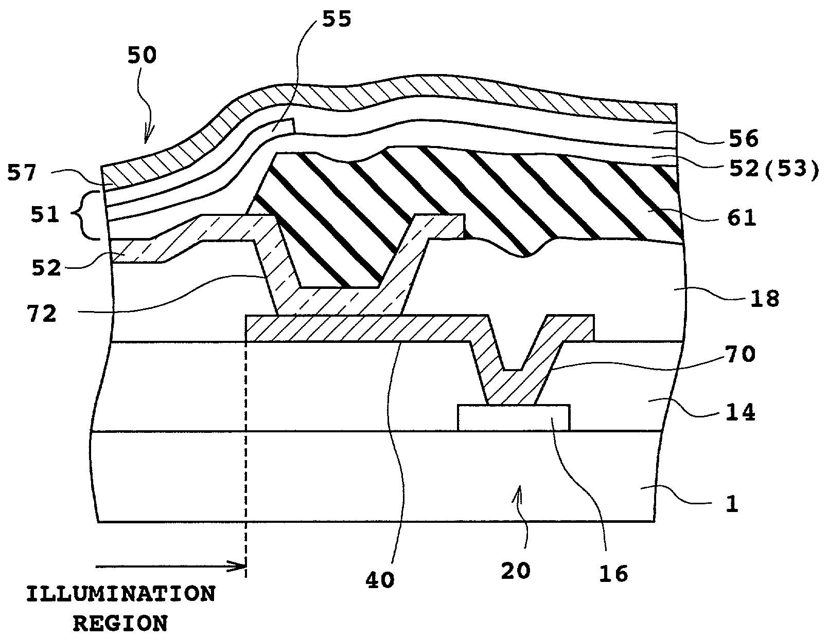
[0085] A second embodiment of the present invention will now be described. In the first embodiment, in order to prevent variation in the illumination brightness among pixels as a result of characteristic variations in the transistor, a compensation thin film transistor having an opposite conductive characteristic as the element driving thin film transistor is provided. In contrast, in the second embodiment, the variation in the illumination brightness among pixels is inhibited by considering the placement of the element driving thin film transistor (second TFT). FIGS. 10A and 10B show an example configuration of one pixel according to the second embodiment. FIG. 10A is a schematic planer view and FIG. 10B is a cross sectional view along the B-B line in FIG. 10A. This structure is shown with the same circuit structure as that of FIG. 1. In these figures, the components corresponding to those in the drawings that are already explained will be referred to by the...

third embodiment

[0103] Third Embodiment

[0104] A method for efficiently connecting a plurality of second TFTs 20 and corresponding organic EL element 50 within one pixel will now be described as a third embodiment of the present invention. As described in the first embodiment and as shown in FIG. 11 of the second embodiment, provision of a plurality of second TFTs 20 between an organic EL element 50 and a power supply line VL within one pixel is advantageous from the viewpoint of improvements in reliability, characteristic, or the like. In a case wherein a plurality of second TFTs 20 are provided within one pixel, as shown in FIG. 11, by respectively connecting the second TFTs 20a and 20b and the organic EL element 50, a current can more reliably be supplied from the power supply line VL to the organic EL element 50 via the second TFTs 20. However, in an organic EL element of the type shown in FIG. 10B in which light from the emissive layer 55 is emitted from a transparent anode 52 to the outside vi...


PUM


Abstract

An EL element (50) having an organic emissive layer or the like between the anode and cathode is used as an element to be driven, and an element driving TFT (20) for controlling the current supplied to the EL element (50) and a compensation thin film transistor (30) having an opposite conductive characteristic as the element driving TFT (20) are provided between the EL element (50) and the power supply line VL. With this structure, variation in the current supplied to each EL element (50) is reduced.

Description

BACKGROUND OF THE INVENTION[0001] 1. Field of the Invention[0002] The present invention relates to an electroluminescent display device, and in particular, to transistors constructing the circuit structure in the pixel section of an electroluminescent display device.[0003] 2. Description of the Related Art[0004] An electroluminescence (hereinafter referred to as EL) display device which uses an EL element which is a self-illuminating element as an illumination element in each pixel has attracted a strong interest as an alternative display device for a display device such as a liquid crystal display device (LCD) and a CRT because the EL display device has advantages such as thin width and low power consumption, in addition to the advantage of being self-illuminating. Such an EL display device has thus been researched.[0005] In particular, there is a high expectation for an active matrix type EL display device in which a switching element such as, for example, a thin film transistor f...

Claims


Application Information

Patent Timeline
IPC IPC(8): G09F9/30H01L51/50G09G3/20G09G3/30G09G3/32H01L21/20H01L21/336H01L27/08H01L27/32H01L29/786H05B33/00
CPCG02F1/13624G09G3/3233G09G2300/0417G09G2300/0426G09G2300/0465G09G2300/0809G09G2300/0842G09G2300/0885G09G2320/0204G09G2320/0233G09G2320/043G09G2330/021H01L27/3244H01L27/3248H01L27/3262H10K59/123H10K59/1213H10K59/12G09G3/30H05B33/00
Inventor ANZAI, KATSUYAKOMIYA, NAOAKI
Owner SANYO ELECTRIC CO LTD
Why Eureka
Try Eureka