
Vertical thin film transistor and method for fabricating the same

a thin film transistor and vertical technology, applied in the field of thin film transistors, can solve the problems of scheme not being able to achieve the reduction of the minimum device size, the amount of required layout area to increase accordingly, and the compensation process not being stable, so as to increase the number of effective current paths, increase the channel length, and enhance the effect of current stability

Active Publication Date: 2019-07-23
INT TECH
View PDF8 Cites 0 Cited by
  • Summary
  • Abstract
  • Description
  • Claims
  • Application Information

AI Technical Summary

Benefits of technology

The top-gate structure enhances current stability and prevents short-channel effects, increasing effective channel length and pixel density, thus improving product yield and accommodating higher pixel densities without increasing layout area.

Problems solved by technology

One factor in the instability of the compensation process is the influence of a threshold voltage (Vth) in a compensation device, or of a circuit voltage drop (IR drop).
However, increases to channel length cause the amount of required layout area to increase accordingly.
The above-mentioned channel scheme cannot achieve the reduced minimum device size.
When the channel length is reduced to less than 2 μm, a serious short-channel effect occurs.
However, the quality of the laser annealing may be reduced due to the bottom-gate TFT structure.
As a result, the electron mobility may be affected.
Although the bottom-gate TFT structure can accommodate the vertical channel scheme to increase the channel length per unit area, the channel conductivity is adversely affected.

Method used


Image

  • Vertical thin film transistor and method for fabricating the same
  • Vertical thin film transistor and method for fabricating the same
  • Vertical thin film transistor and method for fabricating the same

Examples


Embodiment Construction

[0023]The present invention is described in detail with reference to the accompanying drawings that clearly illustrate objectives, technical solution and advantages of the present invention.

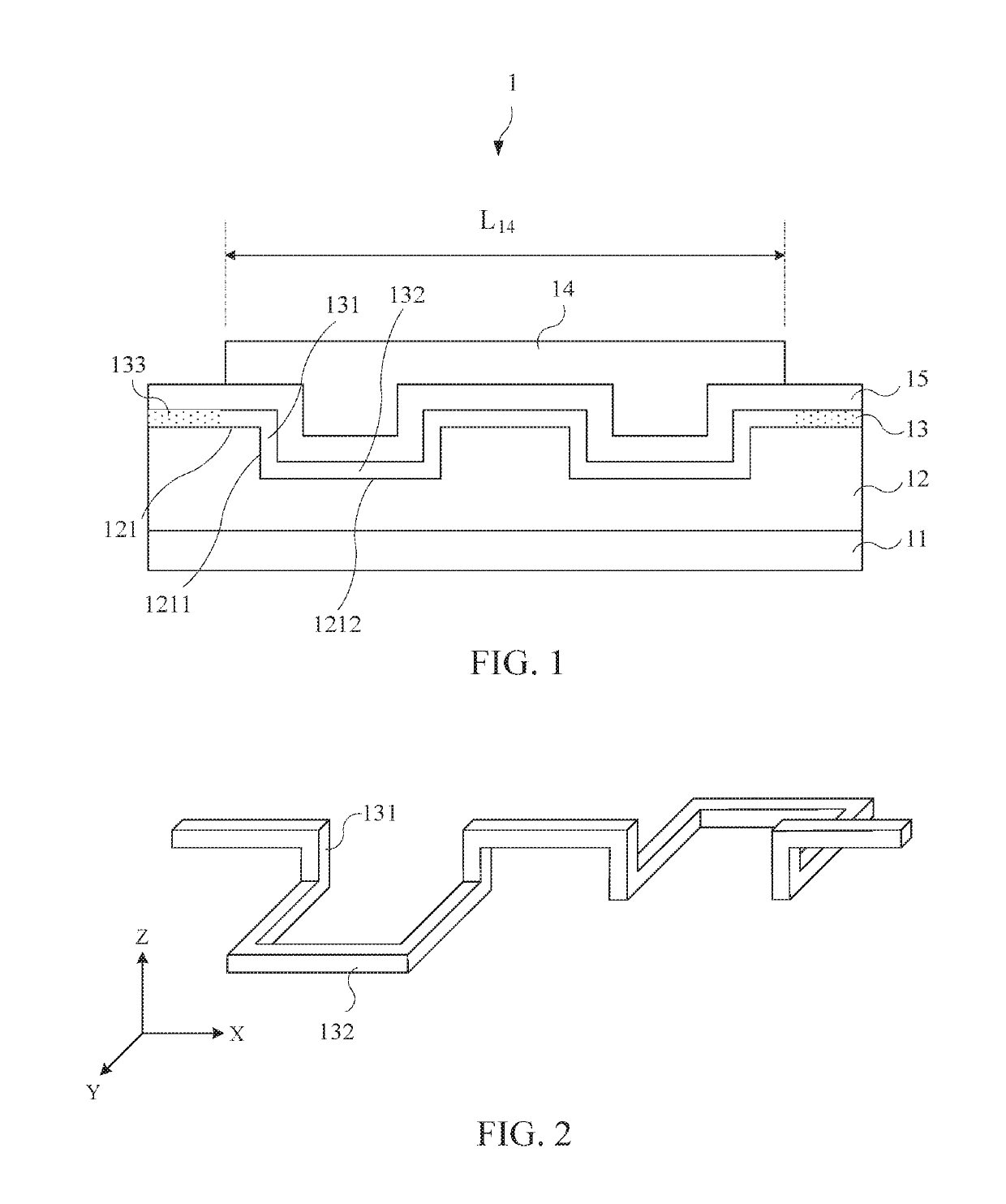
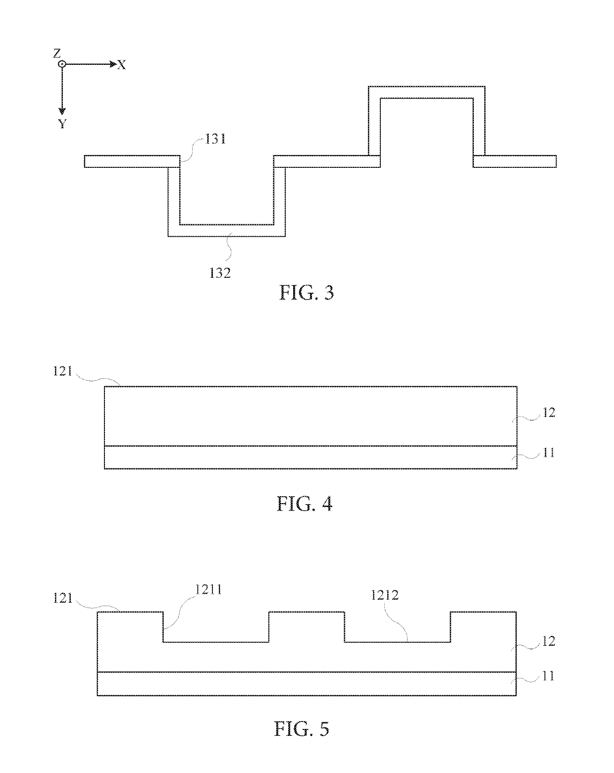
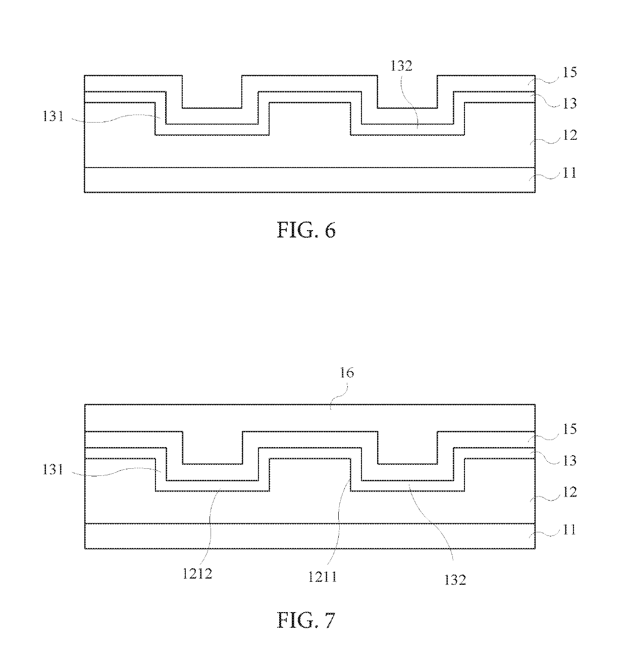
[0024]Referring to FIG. 1, a schematic view of a vertical thin film transistor (VTFT) 1 is shown according to an embodiment of the present invention. One aspect of the present invention provides a VTFT 1. According to an embodiment of the present invention, the VTFT 1 of the present invention includes a substrate 11, a buffer layer 12, a semiconductor layer 13 and a gate electrode 14. The buffer layer 12 is disposed on the substrate 11, and the buffer layer 12 includes a surface 121. The surface 121 has an aperture and the buffer layer 12 has a sidewall 1211 in the aperture. The semiconductor layer 13 is disposed on the surface 121 of the buffer layer 12, and a vertical channel 131 is formed on the sidewall 1211. The gate electrode 14 is disposed on the semiconductor layer 13.

[0025]A width of the...


PUM


Abstract

The present invention discloses a vertical thin film transistor and a method for fabricating the same. A vertical current path is formed in a vertical direction of the thin film transistor, thereby increasing the channel length for a given layout area. The design for the pixel circuit plays an important role in managing the compensation process instability. A relatively long channel is usually needed for driving a thin film transistor so as to improve electrical stability of components, regardless of the compensation circuit used. The present invention provides a vertical thin film transistor having a top gate, such that a current path is formed in the Z direction in addition to the current paths in the X-Y direction. Such scheme increases the effective channel length for a given area, thereby reducing the required layout area. Also, the short-channel effect can be reduced for a gate length of 2 μm.

Description

PRIORITY CLAIM AND CROSS-REFERENCE[0001]This application claims priority to TW Patent Application Serial No. 105125618 filed Aug. 11, 2016, the disclosure of which is hereby incorporated by reference in its entirety.TECHNICAL FIELD[0002]The present invention relates to a thin film transistor, and particularly,to a vertical thin film transistor having a top gate structure with a vertical channel.BACKGROUND[0003]As display technology evolves, the pixel circuit plays an increasingly important role in managing the instability of the compensation process of the active matrix organic light-emitting diode (AMOLED) display technology. One factor in the instability of the compensation process is the influence of a threshold voltage (Vth) in a compensation device, or of a circuit voltage drop (IR drop). A relatively long channel is needed in designing a driving thin film transistor (TFT) to improve the electrical stability of devices. An S-type or V-type structure with a channel length of mor...

Claims


Application Information

Patent Timeline
Patent Type & Authority Patents(United States)
IPC IPC(8): H01L29/78H01L29/417H01L29/786H01L29/423H01L29/66
CPCH01L29/78642H01L29/41733H01L29/42384H01L29/78696H01L29/66787H01L29/785H01L29/78603H01L29/6675H01L29/0684H01L29/66666
Inventor YAN, CHIN-RUNG
Owner INT TECH
Learn More