
Apparatus and method for thin film deposition

a technology of apparatus and thin film, applied in the direction of coating, chemical vapor deposition coating, metallic material coating process, etc., can solve the problems of deteriorating the uniformity and composition of thin film deposited on the substrate, affecting the chemical source gas, and easy heating of shower heads by heaters

Inactive Publication Date: 2002-07-04
JUSUNG ENG
View PDF5 Cites 137 Cited by
  • Summary
  • Abstract
  • Description
  • Claims
  • Application Information

AI Technical Summary

Problems solved by technology

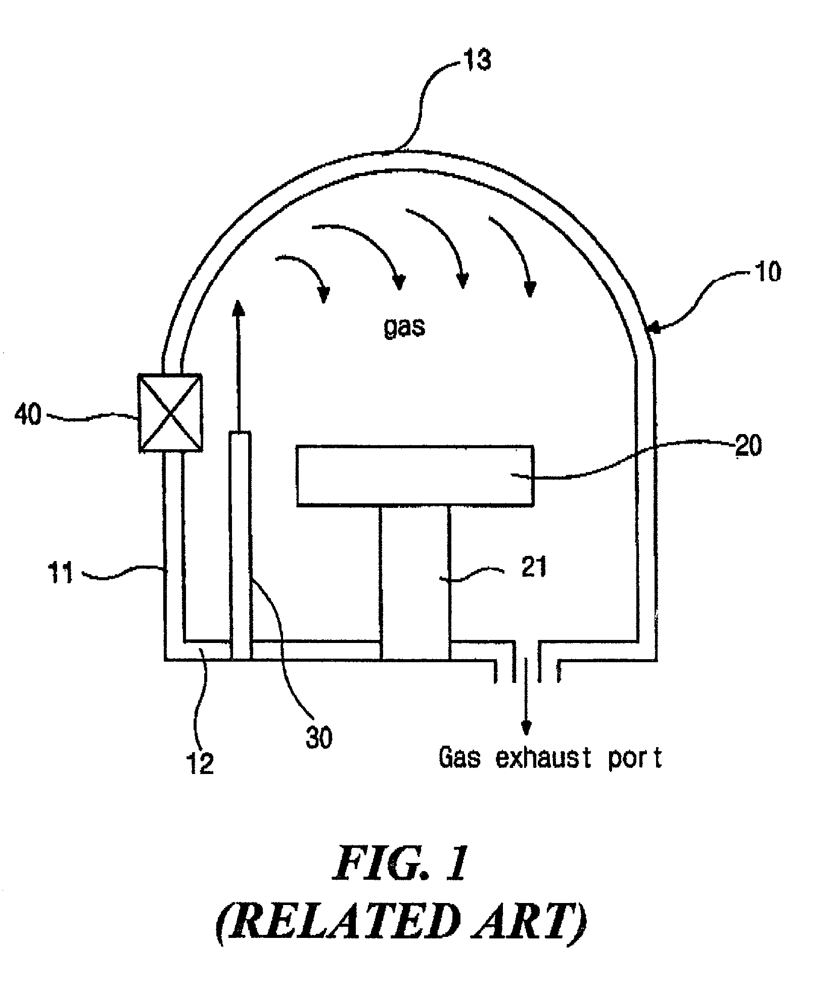
Additionally, since the dispersed chemical source gas delivers a by-product of reaction and a small amount of reactants, which are also accumulated in the gas-dispersing holes, upon the substrate, the by-product and reactants act as impurities in the thin film, thereby deteriorating the uniformity and composition of the thin film deposited on the substrate.
Furthermore, since the shower head is adjacent to a heater applying heat to the substrate, the shower head is easily heated by the heater and the chemical source gas is adversely affected by the heater.
Adopting the cooling system, however, makes the shower head's configuration more confusing.
Also, since the shower heads have different structures and configurations depending on their manufacturers, it is difficult to substitute one thing for another.
However, there are still some problems in the deposited thin film.
Additionally, a large amount of chemical source gas is required to form the thin film, thereby increasing the production cost.
In the meantime, when depositing the thin film using a conventional Chemical Vapor Deposition (CVD), it is impossible to obtain the thin film having an impurity density within a allowable limit and to make the thin film has a thickness of less than several nanometer.
From the result of this density disparity over the substrate, one portion of substrate adjacent to the inflow duct has a thicker thin film rather than the other portion of substrate adjacent to the outflow duct, thereby causing non-uniformity in thickness of the thin film.
Therefore, it takes long time to form the thin film having the uniform thickness, and it is very difficult to obtain even thin film if the reaction chamber is not purged.

Method used


Image

  • Apparatus and method for thin film deposition
  • Apparatus and method for thin film deposition
  • Apparatus and method for thin film deposition

Examples


Embodiment Construction

[0037] Reference will now be made in detail to illustrated embodiment of the present invention, examples of which are shown in the accompanying drawings. Wherever possible, the same reference numbers will be used throughout the drawings to refer to the same or like parts.

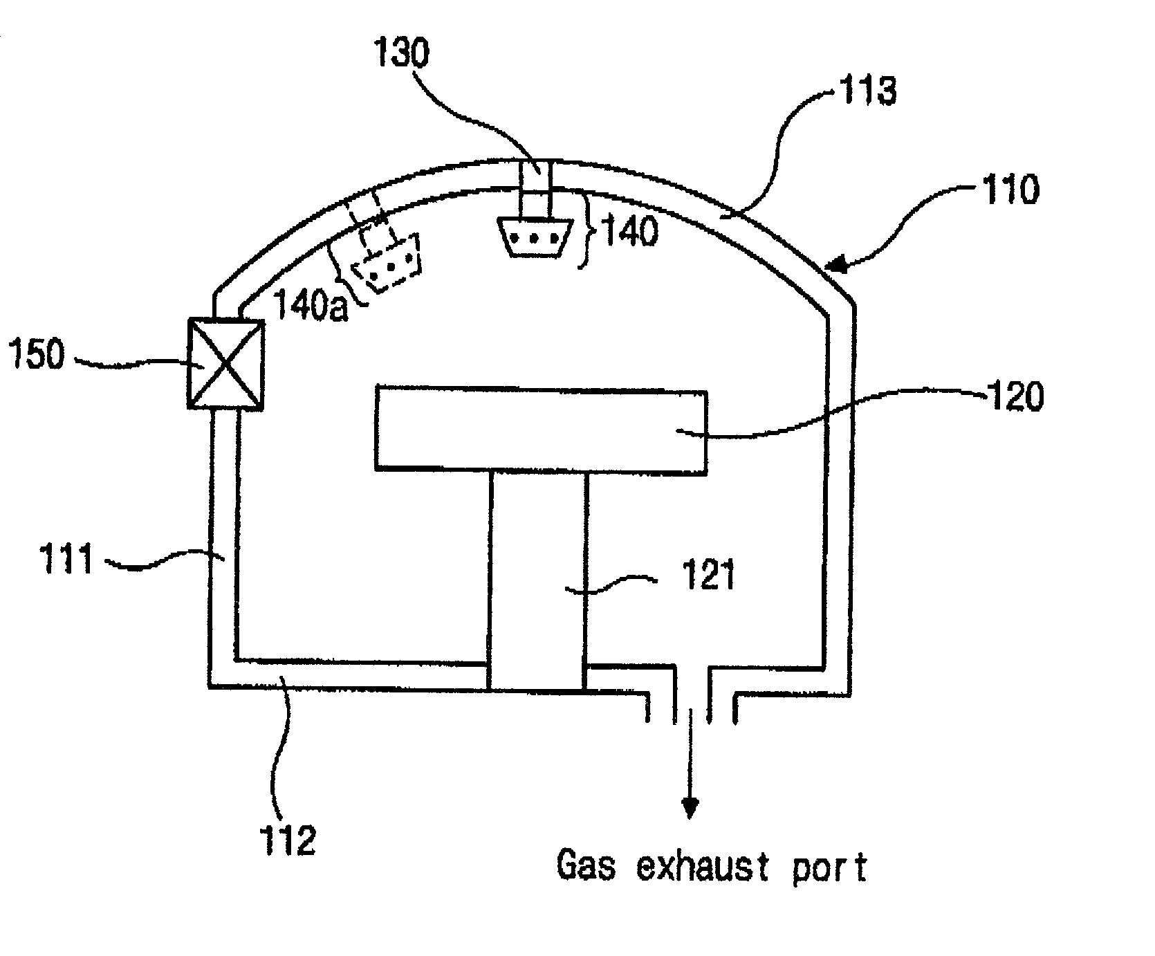
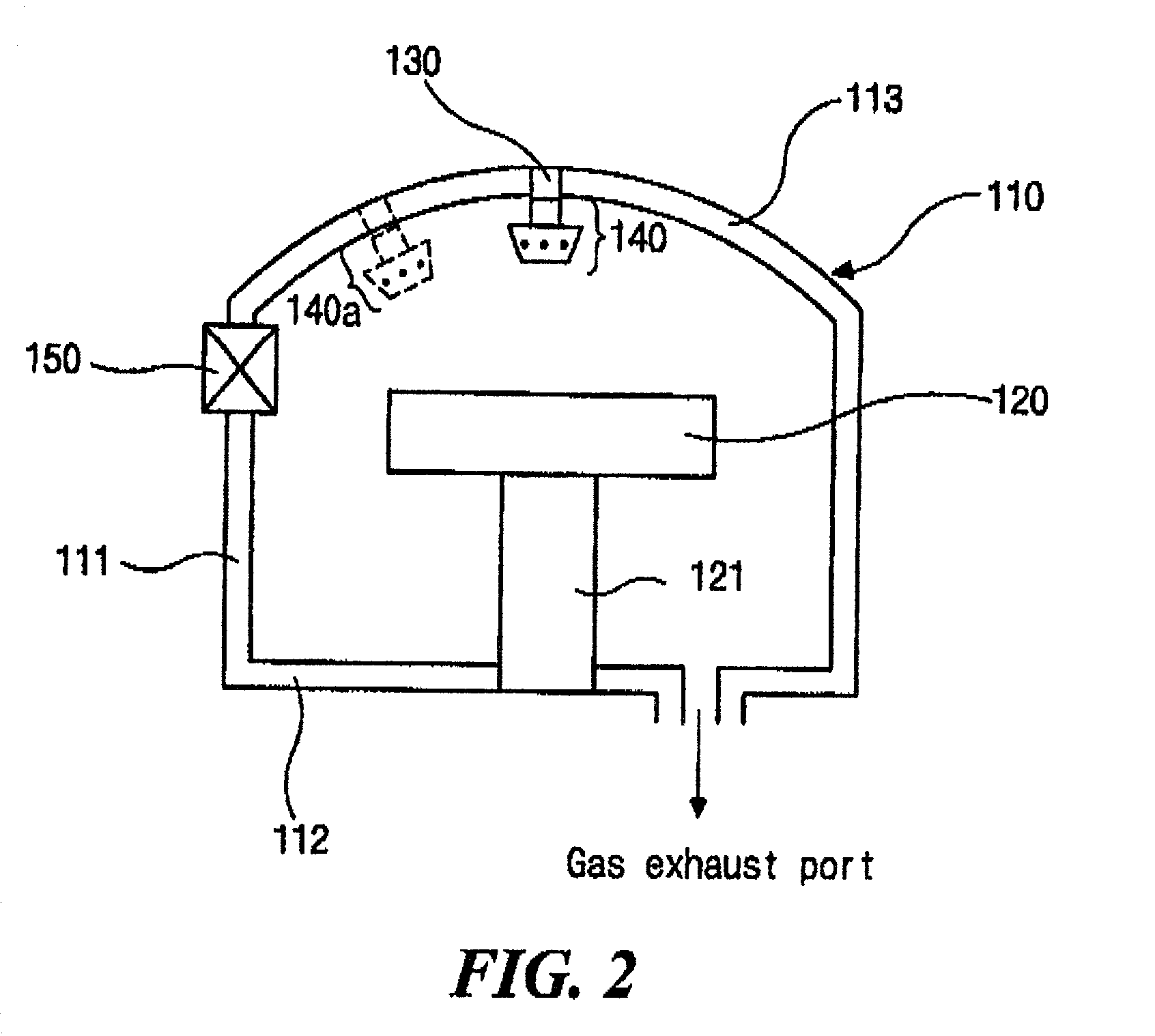
[0038] In the present invention, a distributor having a plurality of injection holes is connected to an injector such that a chemical source gas is spouted through the plurality of injection holes. The chemical source gas from the gas injector is thus evenly diffused in the reaction chamber, thereby forming a uniform thin film upon a substrate. Further, since the Atomic Layer Deposition (ALD) method is employed in the present invention to form the thin film, a super-thin film is obtained with a uniform composition. The detailed explanation will be followed hereinafter.

[0039] FIG. 2 shows a schematic sectional view illustrating a thin film deposition apparatus having a distributor according to a present invention. As...


PUM

PropertyMeasurementUnit
angleaaaaaaaaaa
thicknessaaaaaaaaaa
thicknessesaaaaaaaaaa

Abstract

The apparatus for forming a thin film includes a reaction chamber having a top portion, a sidewall portion and a bottom portion; a gas injector penetrating the top portion and letting a source element pass therethrough; a distributor connected to the gas injector, wherein a plurality of injection holes are formed in the distributor and the source element is injected through the plurality of injection holes; and u substrate heating member positioned in a reaction space defined by the top, bottom and sidewall portions of the reaction chamber, and arranged below the distributor.

Description

[0001] This application claims the benefit of Korean Patent Application No. 2000-65873, filed on Nov. 7,2000, under 35 U.S.C. .sctn.119, the entirety of which is hereby incorporated by reference.BACKROUND OF THE INVENTION[0002] 1. Field of the Invention[0003] This invention relates to a semiconductor device manufacturing apparatus. More particularly, it relates to an apparatus and method for depositing a thin film.[0004] 2. Description of Related Art[0005] The semiconductor devices, such as a memory IC (integrated circuit) and other logic elements, are generally fabricated by repeated depositing and patterning processes. When fabricating the semiconductor devices at the same condition, a thickness uniformity of the deposited thin film should be less than 5% in order to make all the semiconductor devices have an equal property. However, since the highly integrated and finely integrated circuits of semiconductor devices have recently been required, the thickness uniformity of thin fil...

Claims


Application Information

Patent Timeline
Patent Type & Authority Applications(United States)
IPC IPC(8): C23C16/40C23C16/44H01L21/20C23C16/455
CPCC23C16/403C23C16/45544C23C16/45563H01L21/20
Inventor PARK, CHANG-SOOPARK, SANG-GEECHOI, JUNG-HWANCHUNG, BO-SHINOH, SANG-YOUNGLEE, EUNG-SOO
Owner JUSUNG ENG
Learn More