Method for preparing doped ZnO-based film through magnetron sputtering

A magnetron sputtering and thin film technology, applied in sputtering coating, metal material coating process, vacuum evaporation coating, etc., can solve the problems of increasing research cost, lack of doping means, and limiting flexible adjustment of thin film components , to achieve the effect of low cost, controlled doping amount and easy operation

Inactive Publication Date: 2010-07-07
SHENZHEN UNIV
View PDF0 Cites 25 Cited by
  • Summary
  • Abstract
  • Description
  • Claims
  • Application Information

AI Technical Summary

Problems solved by technology

However, there is still a lack of effective doping methods for preparing oxide films by magnetron sputtering technology.
Usually, sputtering grows a film with a specific composition, and it is necessary to prepare a corresponding sputtering target in advance. If a film with a different composition is prepared, a series of corresponding targets need to be prepared. Not only increases the cost of research, but also limits the flexible adjustment of film components

Method used


Image

  • Method for preparing doped ZnO-based film through magnetron sputtering
  • Method for preparing doped ZnO-based film through magnetron sputtering
  • Method for preparing doped ZnO-based film through magnetron sputtering

Examples


Embodiment 1

[0046] Embodiment 1—A high-purity Al target is used as a dopant source to grow an AZO film on a quartz substrate.

[0047] Firstly, Al-doped ZnO thin film (AZO) is prepared by alternately magnetron sputtering ZnO and Al targets using sub-molecular layered doping technology, and is annealed at 400-800°C for 30-60 minutes in an air atmosphere. The growth conditions are:

[0048]

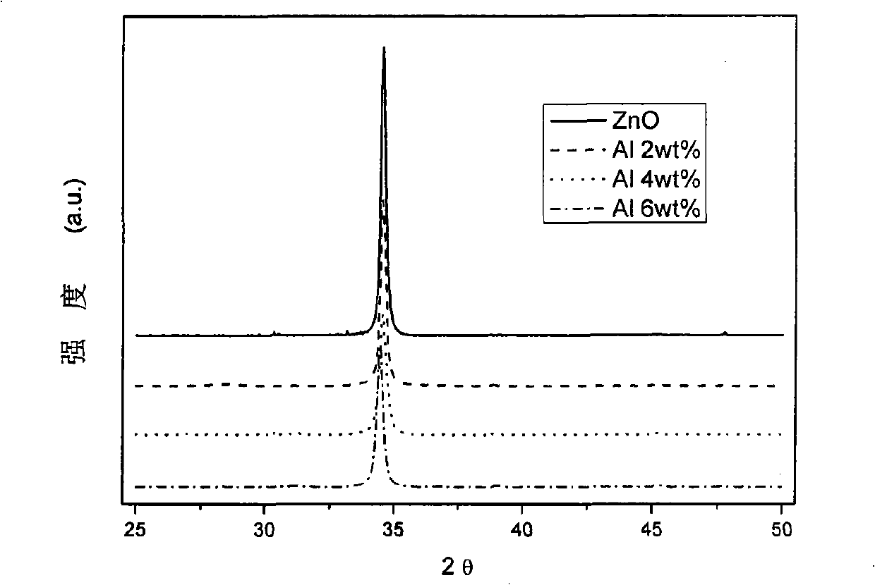
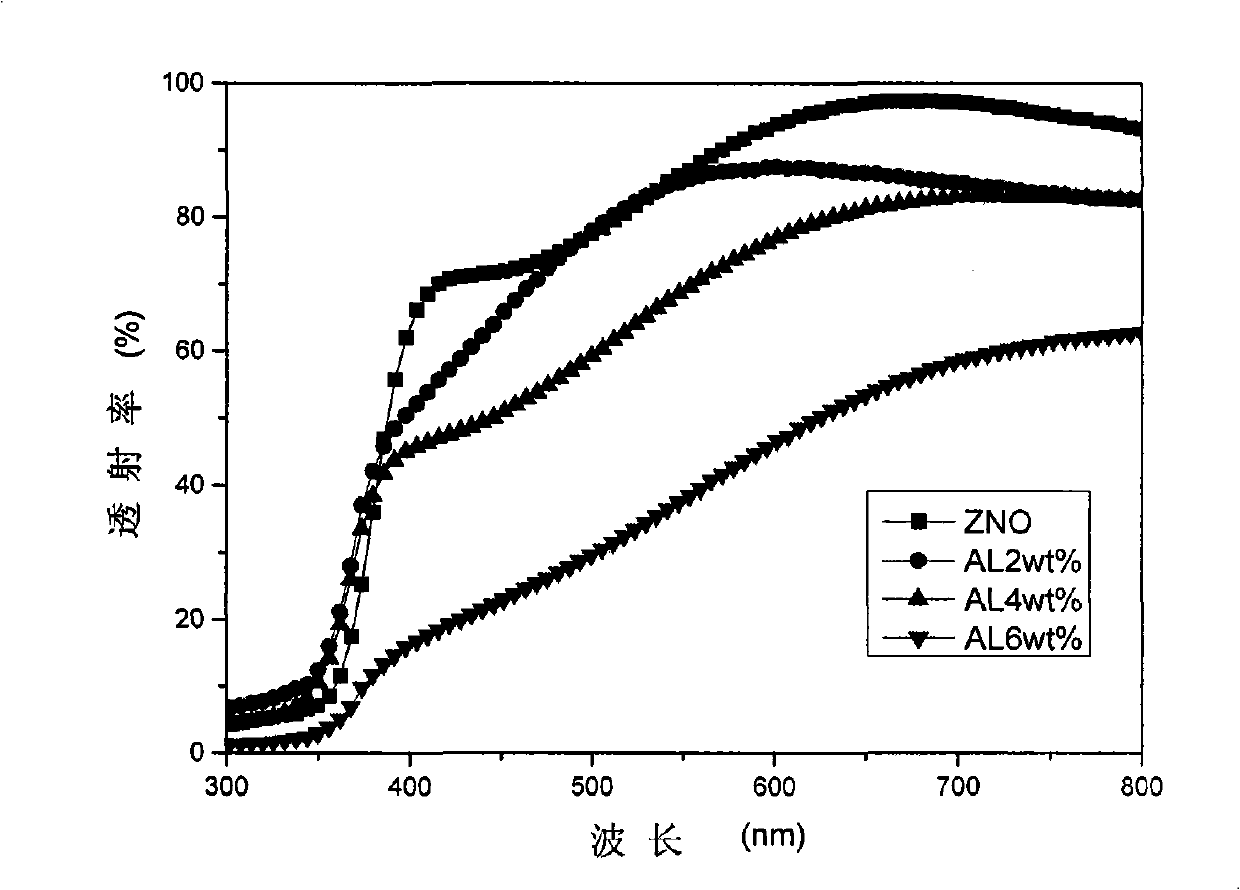
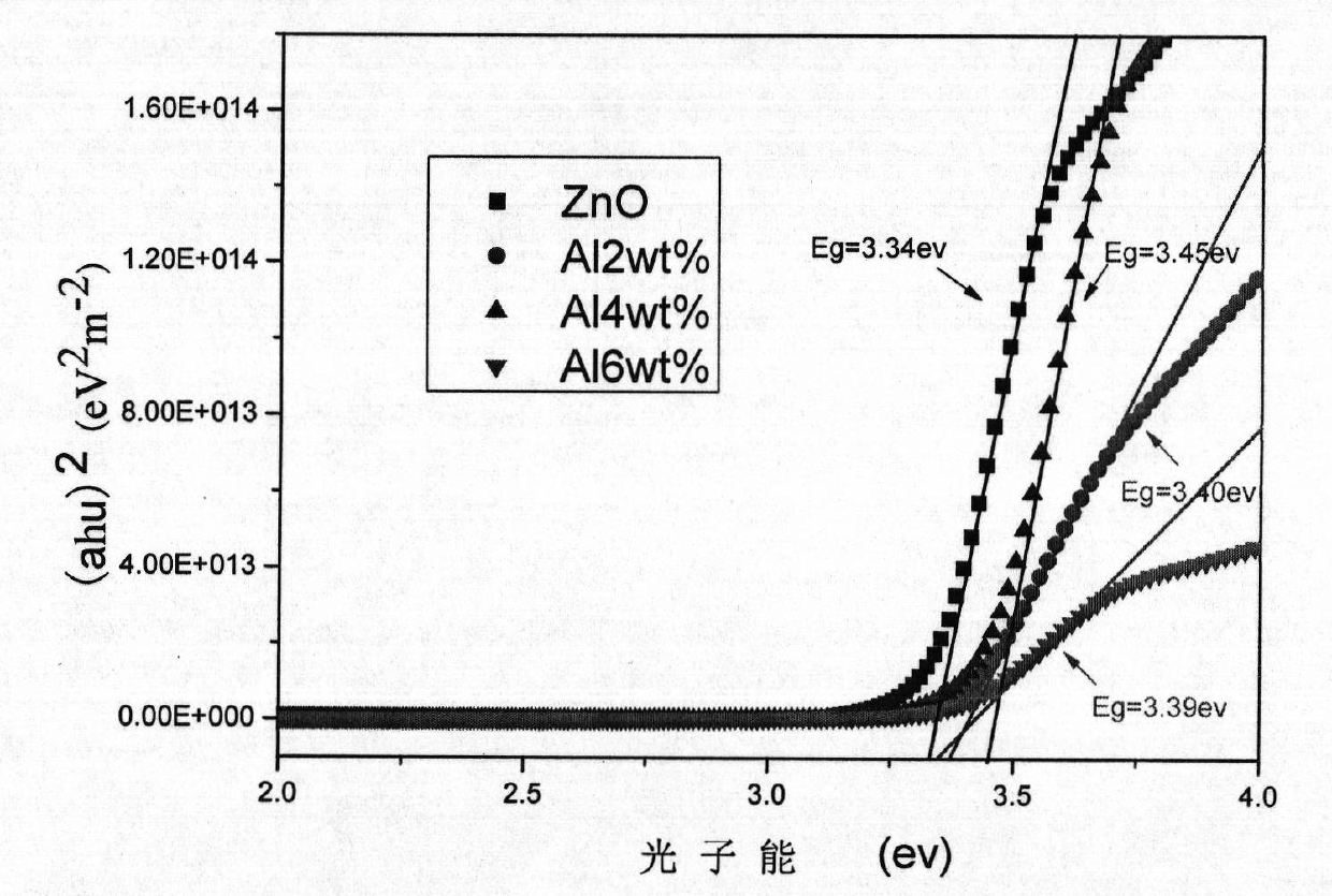
[0049] By changing the sputtering time of the Al target and controlling the content of doped Al (0-6wt%), a good transparent conductive film (TCO) is prepared. After annealing at 400°C, the crystalline quality of the film was improved, and the XRD results showed that all the films had only (002) diffraction peaks, with obvious C-axis preferred orientation, see Picture 1-1 . The average transmittance of the film exceeds 80% in the visible range, see Figure 1-2 . Through the fitting of the ellipsometric spectrum, the optical constant spectrum and film thickness of the AZO thin film sample are giv...

Embodiment 2

[0050] Example 2—Using high-purity Co as a dopant source target, a ZnO:Co(ZCO) film was grown on a Si substrate.

[0051] Firstly, the Co-doped ZnO thin film (ZCO) is prepared by alternately sputtering ZnO and Co targets using submolecular layered doping technology, and is annealed at 400-800°C for 30-60 minutes in a vacuum atmosphere. The growth conditions are:

[0052]

[0053]

[0054] The XRD test results show that the (002) crystal planes of ZCO films with different Co doping amounts have a strong diffraction peak, and their 2θ are very close to the diffraction peaks of pure ZnO crystals, indicating that all ZCO films have c-axis preference orientation, see diagram 2-1 . The depth spectrum of each atom in the ZCO film measured by XPS shows that the layered doping technology is an effective film doping method. The content of Co element on the surface of the film is slightly higher than that in the interior, but the overall content of Co in the film is The distrib...

Embodiment 3

[0055] Example 3—Using a high-purity Mg target as a dopant source to grow Mg on a quartz substrate x Zn 1-x O alloy film.

[0056] Mg-doped ZnO films (Mg x Zn 1-x O), the samples were all annealed at a high temperature of 800° C. for 30 minutes in a nitrogen atmosphere. The growth conditions are:

[0057]

[0058]

[0059] Studies have shown that when the Mg component is low, all Mg x Zn 1-x The O thin film has a ZnO-like (0002) diffraction peak, with an obvious C-axis preferred orientation, and the film has a hexagonal single-phase structure; Similar to MgO(200) diffraction peaks, the sample is a mixed phase of hexagonal phase and cubic phase Figure 3-1 ; In the visible region, the average transmittance of the film exceeds 85%, see Figure 3-2 . With the increase of Mg composition, the transmittance decreases slightly; when the Mg composition is low, the absorption edge will blue shift with the increase of oxygen content, annealing temperature and Mg compositi...


PUM

PropertyMeasurementUnit
transmittivityaaaaaaaaaa

Abstract

The invention provides a method for doping and growing ZnO-based film through magnetron sputtering. The method comprises the following steps: placing a substrate in the reaction chamber of a magnetron sputtering device, vacuumizing the reaction chamber to lower than 1*10<-4>Pa; separately placing ZnO target and doped source element target on the radio frequency target position and DC or electromagnetic target position of the turntable of the reaction chamber, introducing oxygen and argon, which are used as sputtering atmosphere, in a buffer chamber, fully mixing in the buffer chamber, introducing the mixed gas in a vacuum reaction chamber, performing sputtering growth when the pressure is 1-3Pa and the temperature of the substrate is below the room temperature; selecting a sample position and adjusting the sputtering times of the radio frequency target position and DC or electromagnetic target position through a preset program to alternately grow ZnO films and doped element layers; and after the growth placing the doped ZnO-based film in vacuum, air or nitrogen atmosphere to anneal for 30-60 minutes at 400-800 DEG C.

Description

technical field [0001] The invention belongs to the technical field of semiconductor functional thin film materials, in particular to a method for growing a ZnO-based thin film by magnetron sputtering doping. Background technique [0002] ZnO thin film is a semiconductor material with direct bandgap and wide bandgap. The bandgap at room temperature is 3.37eV, and its exciton binding energy is as high as 60meV. It has excellent photoelectric, piezoelectric and dielectric properties, non-toxic, and easy to obtain raw materials. And cheap, it is considered to be the most potential ultraviolet and blue laser luminescent material. Intrinsic ZnO usually exhibits n-type semiconductor characteristics, but its carrier concentration is low. To obtain a sufficiently high carrier concentration, it needs to be doped. In different doping, the representative doping system is: Al-doped ZnO (Al-doped ZnO, referred to as AZO) film, which is considered to be the best substitute for ITO (Sn-do...

Claims


Application Information

Patent Timeline
Patent Type & Authority Applications(China)
IPC IPC(8): C23C14/35C23C14/08C23C14/54C23C14/58
Inventor 马晓翠吕有明柳文军曹培江朱德亮贾芳黄保李清华盛国浩叶家聪向恢复
Owner SHENZHEN UNIV
Why Eureka
Try Eureka