Processing method for forming dislocation-free silicon-on-insulator substrate prepared by implantation of oxygen

Inactive Publication Date: 2002-07-11
IBM CORP
View PDF0 Cites 38 Cited by
  • Summary
  • Abstract
  • Description
  • Claims
  • Application Information

AI Technical Summary

Problems solved by technology

Large amounts of defects in the thin silicon film constitute the main contribution to the yield loss of SOI CMOS.
A majority of defects in SIMOX wafers is due to dislocations.
Dislocations are detrimental to the fabrication of bipolar devices due to the vertical transport of carriers in a bipolar device.
That is, a single dislocation on the act

Method used


Image

  • Processing method for forming dislocation-free silicon-on-insulator substrate prepared by implantation of oxygen
  • Processing method for forming dislocation-free silicon-on-insulator substrate prepared by implantation of oxygen
  • Processing method for forming dislocation-free silicon-on-insulator substrate prepared by implantation of oxygen

Examples


Embodiment Construction

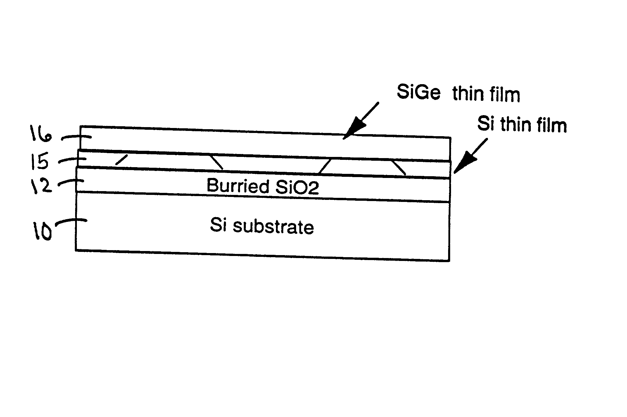
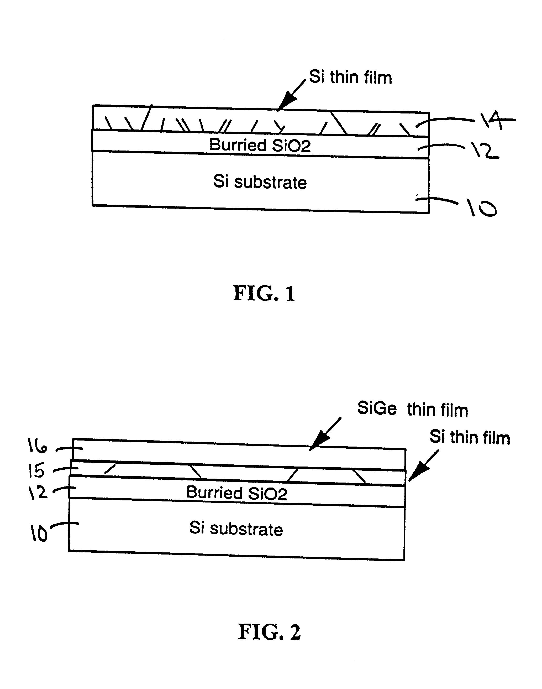
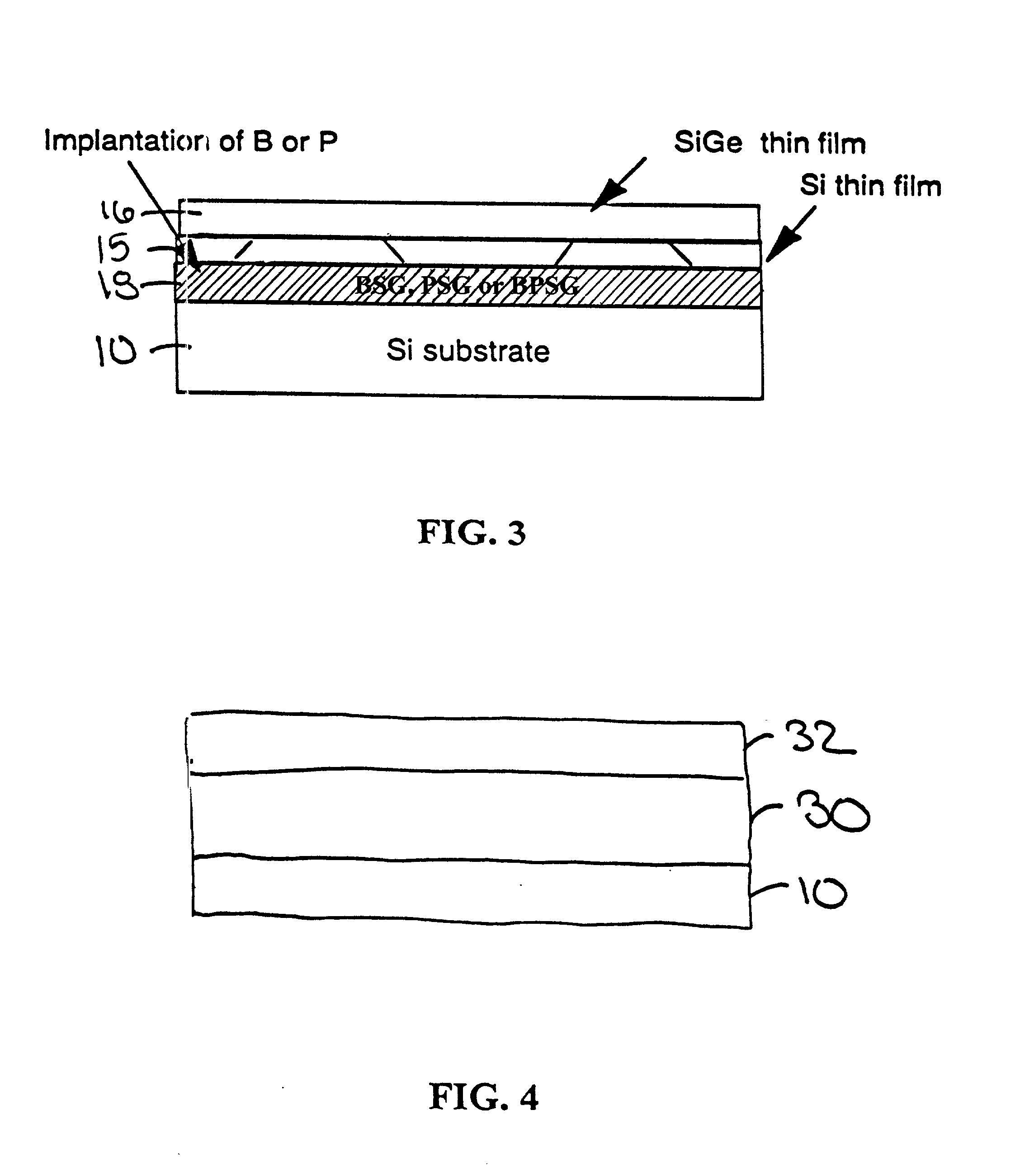
[0024] The present invention provides a unique structure by providing a doped glass layer buried underneath a silicon layer formed by ion implantation over a silicon substrate. This reduces the dislocation density of the top silicon layer and thus provides a better SOI substrate as compared with the prior art such as that shown in FIG. 1.

[0025] To assist the slippage of silicon atoms atop of the buried oxide layer, the re-floating (viscous) temperature of the buried oxide may be reduced. It is well known to one skilled in the art that boron silicate glass (BSG), phosphorous silicate glass (PSG) and boron phosphorous silicate glass (BPSG) have a much lower refloating temperature as compared with silicon dioxide. Depending on the boron or phosphorous concentration, the viscous temperature can go down to 900.degree. C. or even 700.degree. C. At such a low viscous temperature, buried BSG, PSG or BPSG will easily refloat such that the silicon relaxes to become a crystalline structure aft...


PUM

PropertyMeasurementUnit
Structureaaaaaaaaaa
Semiconductor propertiesaaaaaaaaaa
Dislocation densityaaaaaaaaaa

Abstract

A SIMOX semiconductor structure is provided that may include a silicon substrate, a doped glass layer formed on the silicon substrate by ion implantation and a silicon layer formed on the silicon substrate. Ion implantation may form the doped glass layer to reduce the dislocation density of the silicon layer.

Description

[0001] 1. Field of the Invention[0002] The present invention generally relates to reducing the dislocation density in silicon-on-insulator (SOI) materials for use in semiconductor applications.[0003] 2. Description of the Related Art[0004] Silicon-on-insulator (SOI) substrates prepared by ion implantation are called SIMOX wafers. SIMOX substrates have a thin silicon layer situated on top of a buried oxide formed by oxygen implantation. SIMOX wafers are currently used for advanced SOI CMOS technology. Large amounts of defects in the thin silicon film constitute the main contribution to the yield loss of SOI CMOS. A majority of defects in SIMOX wafers is due to dislocations. Dislocations are detrimental to the fabrication of bipolar devices due to the vertical transport of carriers in a bipolar device. That is, a single dislocation on the active area may result in high leakage and destroy the device.[0005] The dislocation density of SIMOX wafers prepared by conventional methods is on ...

Claims


Application Information

Patent Timeline
IPC IPC(8): C23C14/48H01L21/02H01L21/265H01L21/762H01L27/12
CPCH01L21/76243
Inventor HUANG, FENG-YI
Owner IBM CORP
Why Eureka
Try Eureka