Apparatus for polishing a semiconductor wafer and method therefor

a technology of semiconductor wafers and polishing heads, which is applied in the direction of grinding drives, manufacturing tools, lapping machines, etc., can solve the problems of affecting the polishing effect of the polishing head,

Inactive Publication Date: 2002-07-25
SAMSUNG ELECTRONICS CO LTD
View PDF0 Cites 44 Cited by
  • Summary
  • Abstract
  • Description
  • Claims
  • Application Information

AI Technical Summary

Problems solved by technology

However, the vacuum between the membrane and the wafer is often leaked, such that during transfer, the wafer may be dropped or otherwise harmed.
However, such a polishing head introduces limitations that are shown in FIG. 1, which is a graph illustrating the resulting uneven surface of a wafer.
Portions A and B are relatively over-polished as compared to other portion of the wafer, thereby compromising the uniformity of polishing surface of the wafer.

Method used


Image

  • Apparatus for polishing a semiconductor wafer and method therefor
  • Apparatus for polishing a semiconductor wafer and method therefor
  • Apparatus for polishing a semiconductor wafer and method therefor

Examples


first embodiment

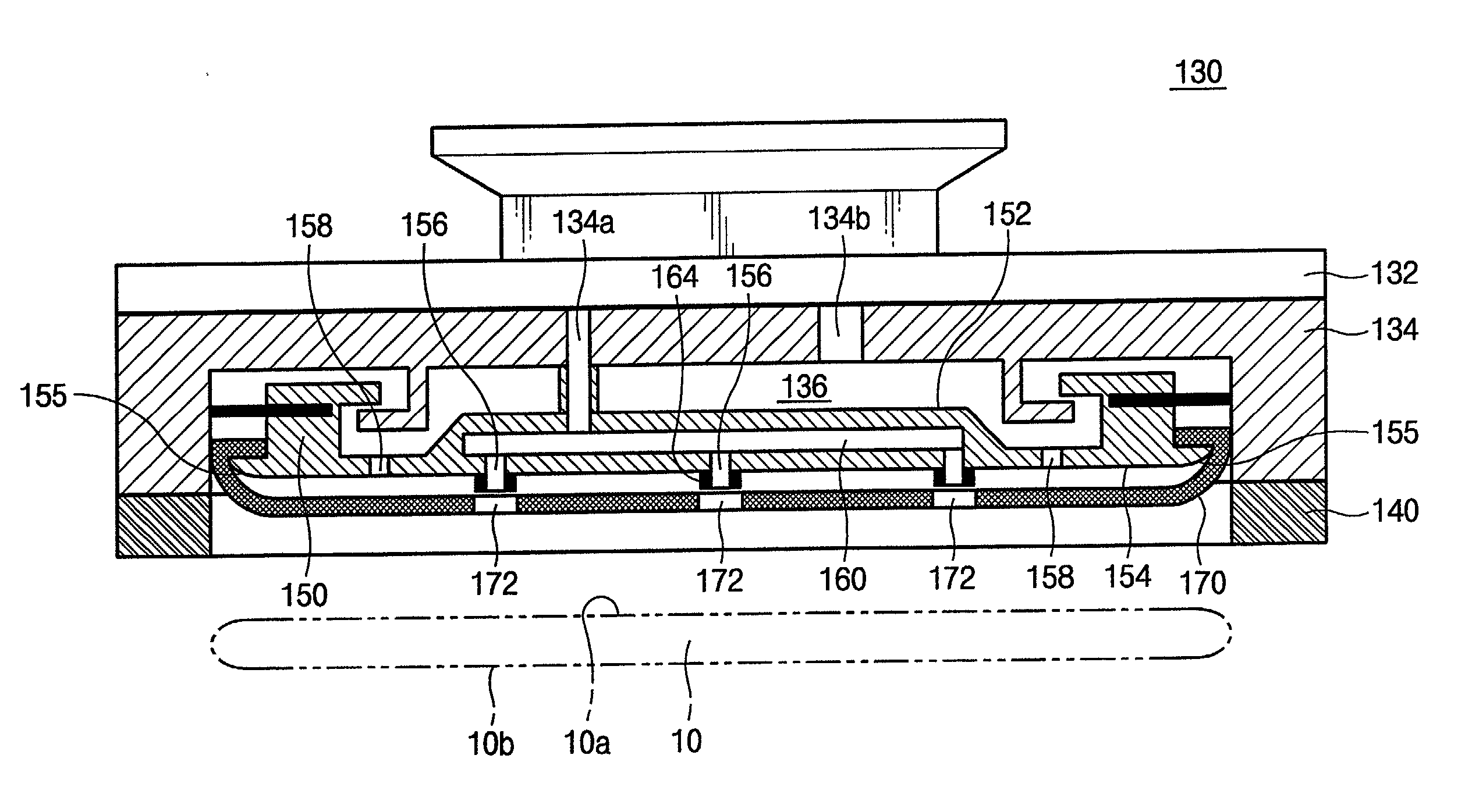
[0046] Referring to FIGS. 3 through 5, a polishing head 130 in accordance with a preferred first embodiment of the present invention includes a manifold 132, a dishshaped carrier 134, a retainer ring 140, a supporter 150 and a flexible membrane 170. The manifold 132 is a component serving to connect the two fluid channels to first and second fluid passages 134a, 134b, as shown in FIG. 5. The supporter 150 disposed in the carrier 134 has an upper surface portion 152, a lower surface portion 154, a plurality of first holes 156, a plurality of second holes 158, and a first chamber 160. The upper surface portion 152 of the supporter 150 forms a second chamber 136 along with an inner surface of the carrier 134. The second chamber 136 communicates with the second fluid passage 134b of the carrier 134 and the second holes 158 formed in the lower surface portion 154 of the supporter 150. The first chamber 160 communicates with the first fluid passage 134a and the first holes 156. The lower ...

embodiment 2

[0061] FIG. 7a and FIG. 7b illustrate cross-sections of a polishing head 130a in accordance with a preferred second embodiment of the present invention. The polishing head 130a of the second embodiment is different than the polishing head 130 of the first embodiment in the sense that the load can be individually controlled at both the supporter 150a and the retainer ring 140. Also, the polishing head 130a has a separate chucking ring for use in moving of the wafer.

[0062] Downward pressure of the retainer ring 140 is controlled by air supplied through a third fluid passage 134c of a manifold 132. For this, a first elastic member 180 is disposed between the manifold 132 and a carrier 134. The elastic member 180 is expanded or compressed by air supplied through the third fluid passage 134c to impose load on the carrier 134. The carrier 134 is coupled with the retainer ring 140 to impose a downward load thereto. The elastic member 180 is composed of synthetic rubber, so that it can be e...

second embodiment

[0066] A wafer polishing process of an apparatus for CMP 100 having a polishing head 130a in accordance with the present invention will now be described. The polishing process comprises the steps of loading a wafer 10 on an abrasive pad 112 of a turntable 114 by means of a polishing head 130a, polishing a front or second surface 10b of the wafer 10 by imposing an air pressure on a membrane 170a, chucking the wafer 10 by means of the polishing head 130a, and unloading the wafer 10 on a stand-by stage (not shown) from the abrasive pad 112 of the turntable 114.

[0067] The steps of the polishing process are explained in detail with reference to the following table.

2 TABLE 2 The first The second The third chamber chamber fluid passage Loading Zero or Vacuum Pressure .fwdarw. zero step vacuum Polishing Pressure Pressure Pressure step Chucking Zero or Vacuum Pressure .fwdarw. zero step vacuum Unloading Any one of Pressure Zero step Pressure, zero, and vacuum (If possible, pressure)

[0068] Re...


PUM

PropertyMeasurementUnit
thicknessaaaaaaaaaa
circumferenceaaaaaaaaaa
shapeaaaaaaaaaa

Abstract

An apparatus for polishing a wafer comprises a supporting portion having an abrasive pad disposed thereon, and a polishing head disposed over the abrasive pad. The polishing head comprises a carrier having at least two fluid passages, a retainer ring disposed on a lower edge of the carrier, forming a space for receiving the wafer, a supporter disposed in the carrier, and a flexible membrane disposed to be in contact with the wafer. The supporter has an upper surface portion, a lower surface portion, a plurality of first holes, a plurality of second holes, and a first chamber. The upper surface portion of the supporter forms a second chamber along with an inner surface of the carrier. The second chamber is in communication with one of the two fluid passages of the carrier and the second holes are formed in a lower surface portion of the supporter to communicate with the second chamber. The first chamber is in communication with the other one of the two fluid passages and the first holes are formed in the lower surface portion of the supporter to communicate with the first chamber. The lower surface portion of the supporter has a flat surface and a chamfered or rounded edge. The membrane disposed to enclose the lower surface portion of the supporter has a plurality of third holes formed at positions corresponding to the first holes to absorb and hold the wafer by vacuum.

Description

[0001] This application relies for priority upon Korean Patent Application No. 2000-69983, filed on Nov. 23, 2000 and Korean Patent Application No. 2001-11055, filed on Mar. 3, 2001, the contents of which are herein incorporated by reference in their entirety.Field of the Invention[0002] The present invention relates to an apparatus for manufacturing a semiconductor wafer and method therefor, and more particularly to an apparatus for polishing a semiconductor wafer and method therefor.Background of the Invention[0003] As the elements incorporated into a semiconductor device are increasingly integrated, the structure of device wires such as gate lines and bit lines continues to become multiple-layered. For this reason, step coverage between unit cells on a semiconductor substrate is increased. To reduce the step coverage between the unit cells, various methods of polishing a wafer have been developed. Among these methods, a chemical-mechanical polishing (CMP) method which planarizes ...

Claims


Application Information

Patent Timeline
Patent Type & Authority Applications(United States)
IPC IPC(8): B24B37/005B24B37/30H01L21/304
CPCB24B37/30B24B37/32H01L21/304
Inventor BOO, JAE-PHILRYU, JUN-GYULEE, SANG-SEONLEE, SUN-WUNG
Owner SAMSUNG ELECTRONICS CO LTD
Why Eureka
Try Eureka