Flat panel display device

a display device and flat panel technology, applied in the field of flat panel display devices, can solve the problems of undesirable electrode pickup sections, a large amount of time and labor, and the system involves a great difficulty in adjusting the tones and luminance of respective panels, so as to avoid the breakage of the bus electrodes

Inactive Publication Date: 2002-08-29
PIONEER CORP
View PDF4 Cites 22 Cited by
  • Summary
  • Abstract
  • Description
  • Claims
  • Application Information

AI Technical Summary

Benefits of technology

0076] The thickness of the first insulating protective films 17a in the above-described embodiment may be set at a value that is similar to or greater than the thickness up to the electron supply layer 12 as shown in FIG. 6, this is not limiting the present invention. For example, breakage of the bus electrodes can be avoided if the films have a thickness that is 5% or more of the thickness of the electron emission sites as shown in FIG. 17. Therefore, the thickness of the first insulating protective films is preferably 5% or more of the thickness of the devices as a whole (about 6 .mu.m) (the upper liming being a thickness that is substantially equal to the height of the device insulator layer 13). The lower limit for the thickness of the first insulating protective films 17a is a thickness which does not cause breakage of the bus electrodes.

Problems solved by technology

The former display system has a very large depth from the front thereof and therefore requires a lot of time and labor to assemble it.
The latter display system involves a great difficulty in adjusting the tones and luminance of respective panels.
Since three sides of panels must be used in the conventional method for picking up FED electrodes as thus described, electrode pickup sections undesirably overlap each other on three sides when they are assembled into a unit.
When panels are assembled into a unit, sides of the panels must be tightly combined with each other, and measures must be taken to prevent any overlap between electrode pickup sections, which makes the assembly process very much difficult.

Method used


Image

  • Flat panel display device
  • Flat panel display device
  • Flat panel display device

Examples


Embodiment Construction

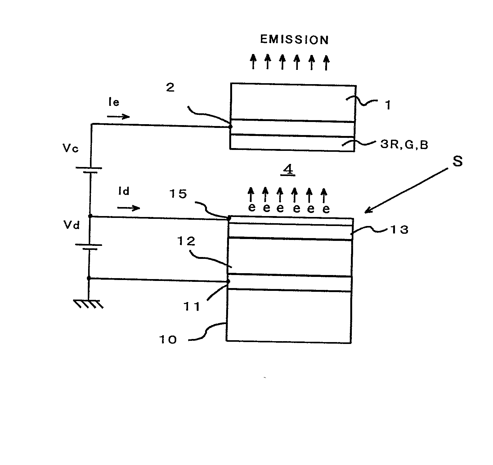
[0078] A flat panel display device was actually fabricated with specifications (1) through (6) as shown below using a sputtering process for film formation and then characteristics of the same were examined. (1) Bottom electrodes: Cr, Cu, and Cr films having thicknesses of 50 nm, 1 .mu.m, and 100 nm, respectively. (2) Semiconductor electron supply layer: Si layer having a thickness of 4 .mu.m. (3) Insulator layer: SiO.sub.x layer having a thickness of 330 nm. (4) Top electrode: Pt film having a thickness of 40 nm. (5) Bus electrodes: Cr, Cu, and Cr films having thicknesses of 50 nm, 1 .mu.m, and 100 nm, respectively. (6) Second external repeating terminals: Cr, Cu, and Cr films having thicknesses of 50 nm, 1 .mu.m, and 100 nm, respectively. (7) First, second, and third insulating protective films: SiO.sub.x films having a thickness of 350 nm.

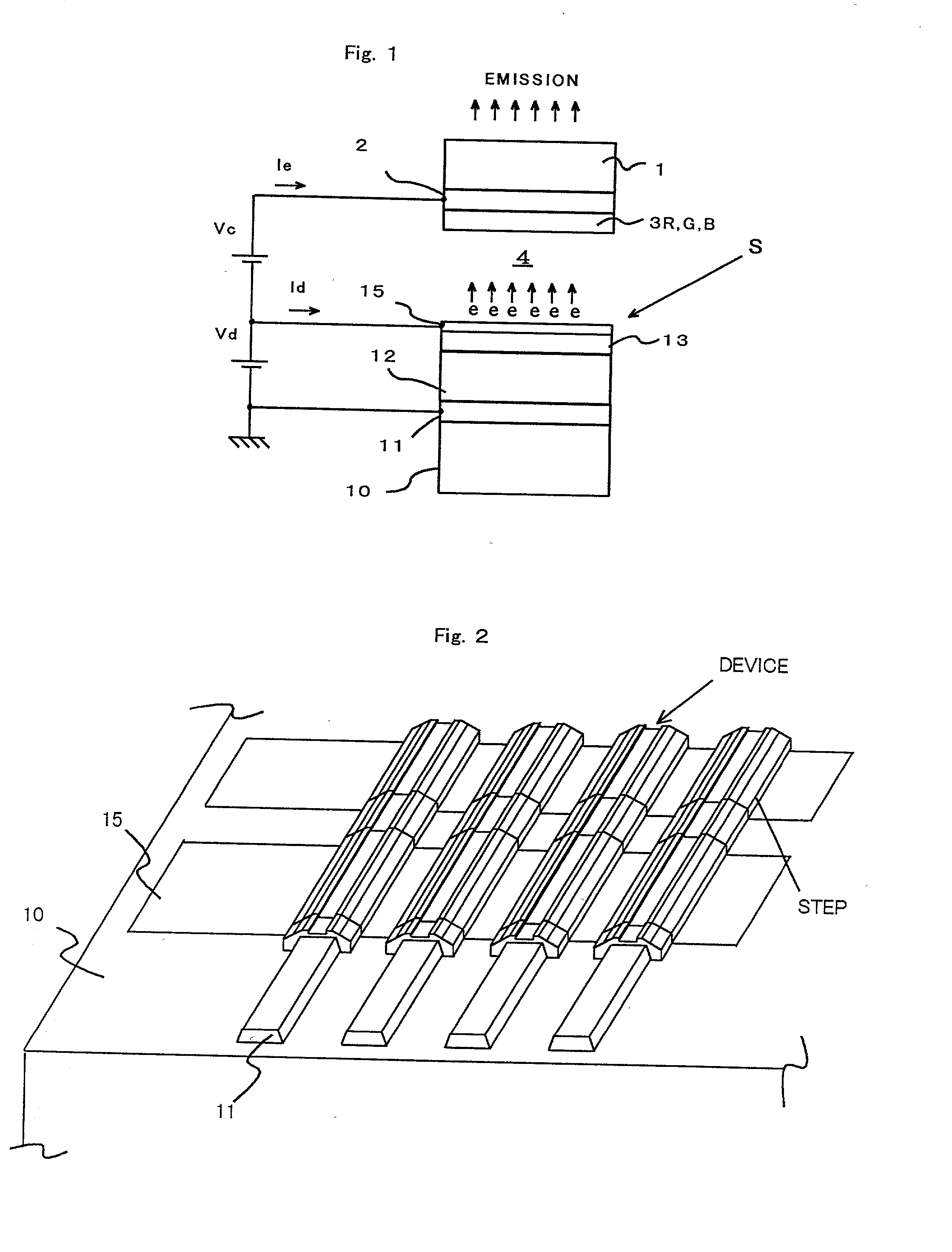
[0079] The bottom electrodes (1) and semiconductor electron supply layers (2) were formed in the form of lines on a glass substrate which had b...


PUM


Abstract

A display device has an emitting region constituted by a plurality of first electrodes provided on a substrate and extending in parallel, a plurality of second electrodes provided on the first electrodes and extending substantially perpendicularly to the first electrodes, and a plurality of emission sites for emitting electrons or light respectively connected to a plurality of intersections between the first and second electrodes and arranged on the substrate and has a peripheral region surrounding the emitting region on the substrate. In this display device, first and second groups of external repeating terminals for the first and second electrodes are collectively provided side by side in a part of the peripheral region.

Description

[0001] 1. Field of the Invention[0002] The present invention relates to a flat panel display device.[0003] 2. Description of the Related Art[0004] There are merchandized products of ultra-large display systems for example a large screen multi-projection system using projection units in which plural projectors such as three CRTs or liquid crystal displays for RGB are arranged in vertical and horizontal directions. A system utilizing plural LED array panels composed flat is also available for the ultra-large display system. The former display system has a very large depth from the front thereof and therefore requires a lot of time and labor to assemble it. The latter display system involves a great difficulty in adjusting the tones and luminance of respective panels. Under such circumstances, there are attracting attentions as promising next generation ultra-large display devices e.g., units consisting of flat panel display devices such as organic electroluminescence devices, and elec...

Claims


Application Information

Patent Timeline
Patent Type & Authority Applications(United States)
IPC IPC(8): G09F9/30H01L51/50H01J1/30H01J1/60H01J11/10H01J17/49H01J29/92H01J31/12H01L27/32H05B33/28
CPCB82Y10/00H01J1/30H01J1/60H01J11/10H01J29/92H01J31/12H01J31/127H01J2201/3125H01J2211/46H01L27/3288H10K59/179
Inventor CHUMAN, TAKASHIYOSHIKAWA, TAKAMASAHATA, TAKUYASAKEMURA, KAZUTOYAMADA, TAKASHINEGISHI, NOBUYASUIWASAKI, SHINGOSATOH, HIDEOYOSHIZAWA, ATSUSHIOGASAWARA, KIYOHIDE
Owner PIONEER CORP
Why Eureka
Try Eureka