Structures, methods, and systems for ferroelectric memory transistors

Inactive Publication Date: 2002-09-19
MICRON TECH INC
View PDF0 Cites 53 Cited by
  • Summary
  • Abstract
  • Description
  • Claims
  • Application Information

AI Technical Summary

Benefits of technology

0008] To address these and other needs, the inventors devised unique ferroelectric gate structures and related fabrications methods. One exemplary gate structure includes a high-integrity silicon oxide insulative layer; a doped titanium-oxide layer; a weak ferroelectric layer; and a control gate. In contrast to the conventional gate structure, this exemplary structure replac

Problems solved by technology

The problem is that the multilayer gate structure forces the insulative layer to withstand a greater portion of voltages applied to the control gate than the ferroelectric layer, even though the ferroelectric, because of its at least 100 times greater permittivity, can withstand greater voltages than the in

Method used


Image

  • Structures, methods, and systems for ferroelectric memory transistors
  • Structures, methods, and systems for ferroelectric memory transistors
  • Structures, methods, and systems for ferroelectric memory transistors

Examples


Embodiment Construction

[0014] The following detailed description, which references and incorporates FIGS. 1-4, describes and illustrates specific embodiments of the invention. These embodiments, offered not to limit but only to exemplify and teach the invention, are shown and described in sufficient detail to enable those skilled in the art to implement or practice the invention. Thus, where appropriate to avoid obscuring the invention, the description may omit certain information known to those of skill in the art.

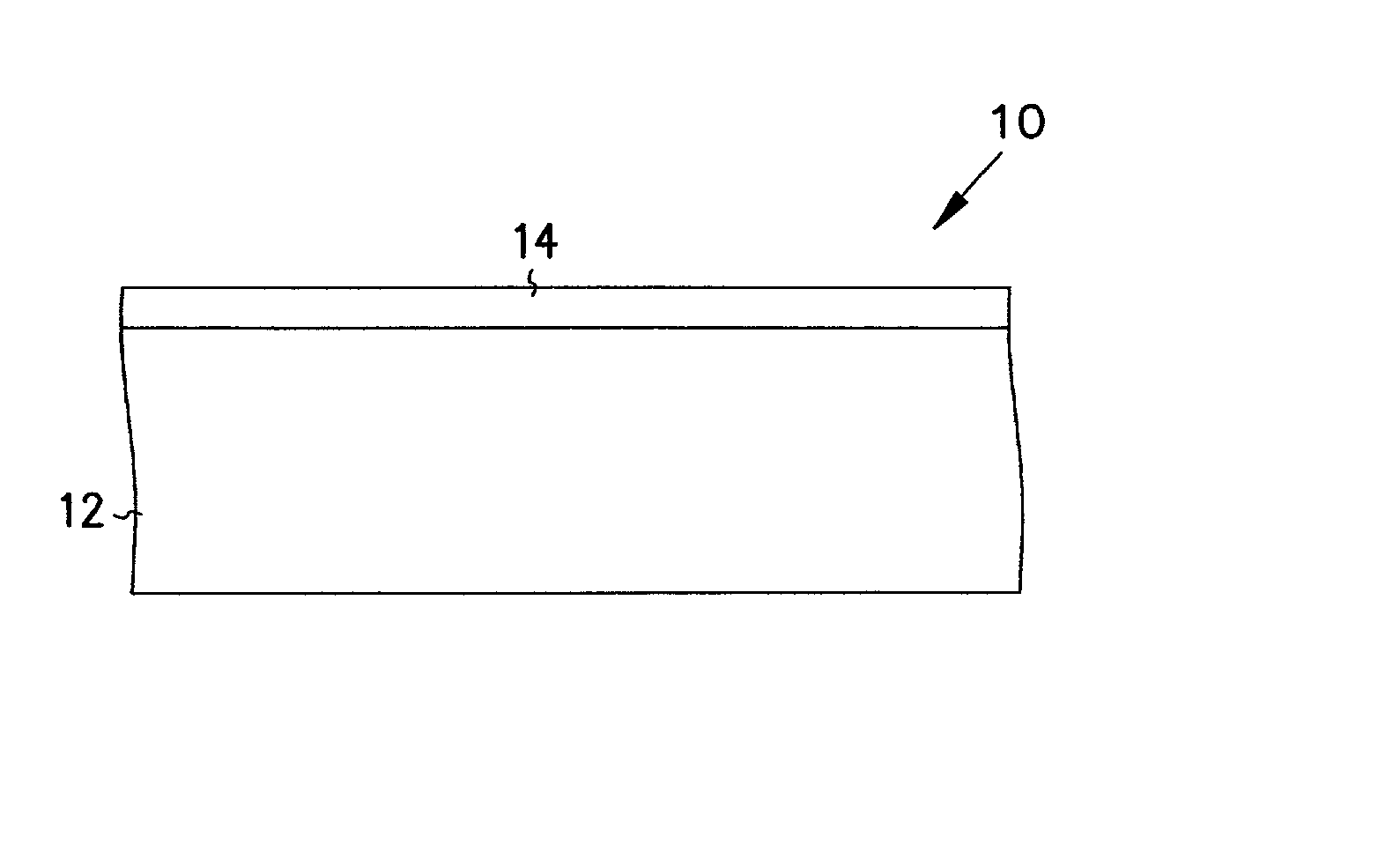
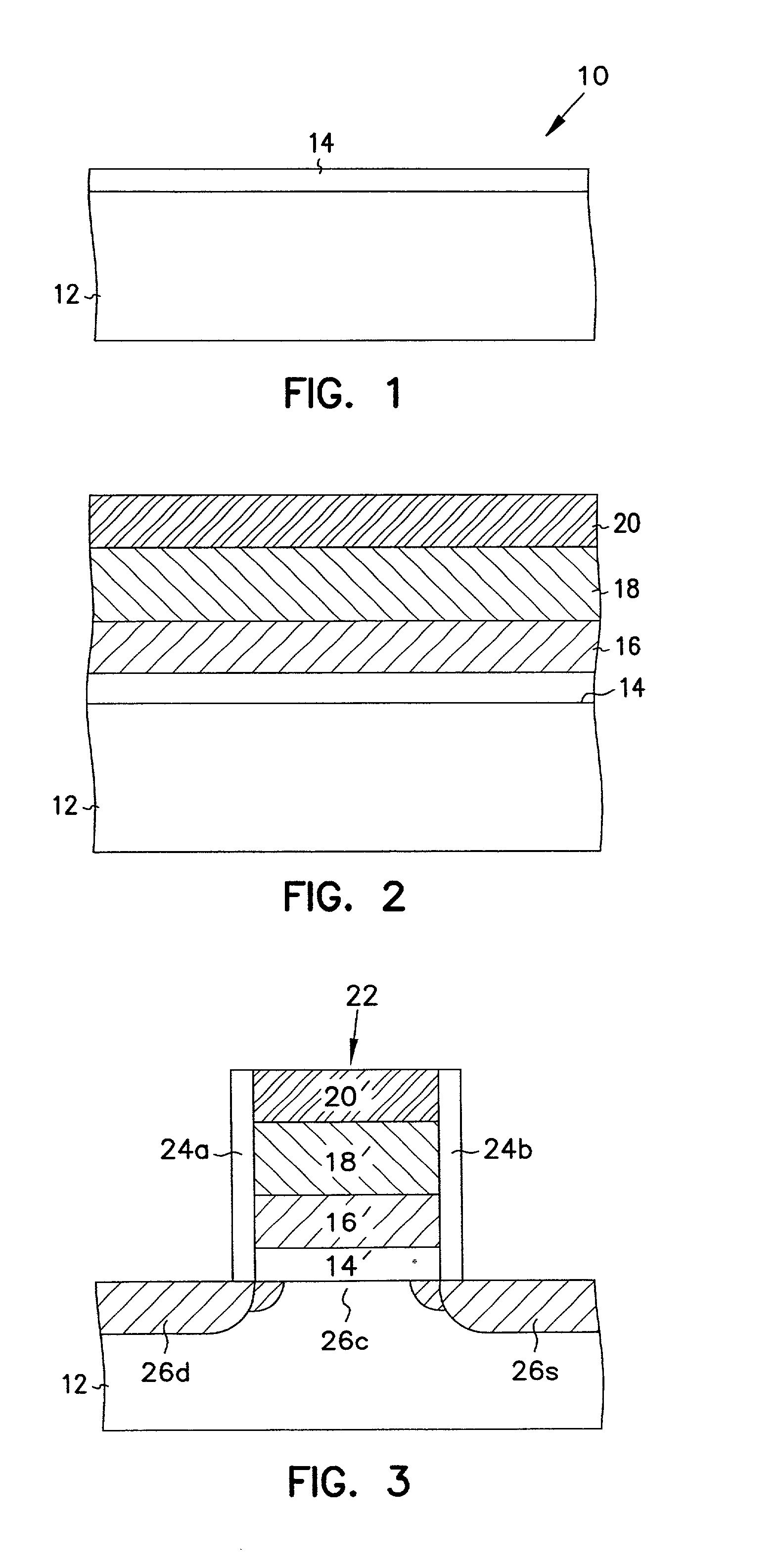
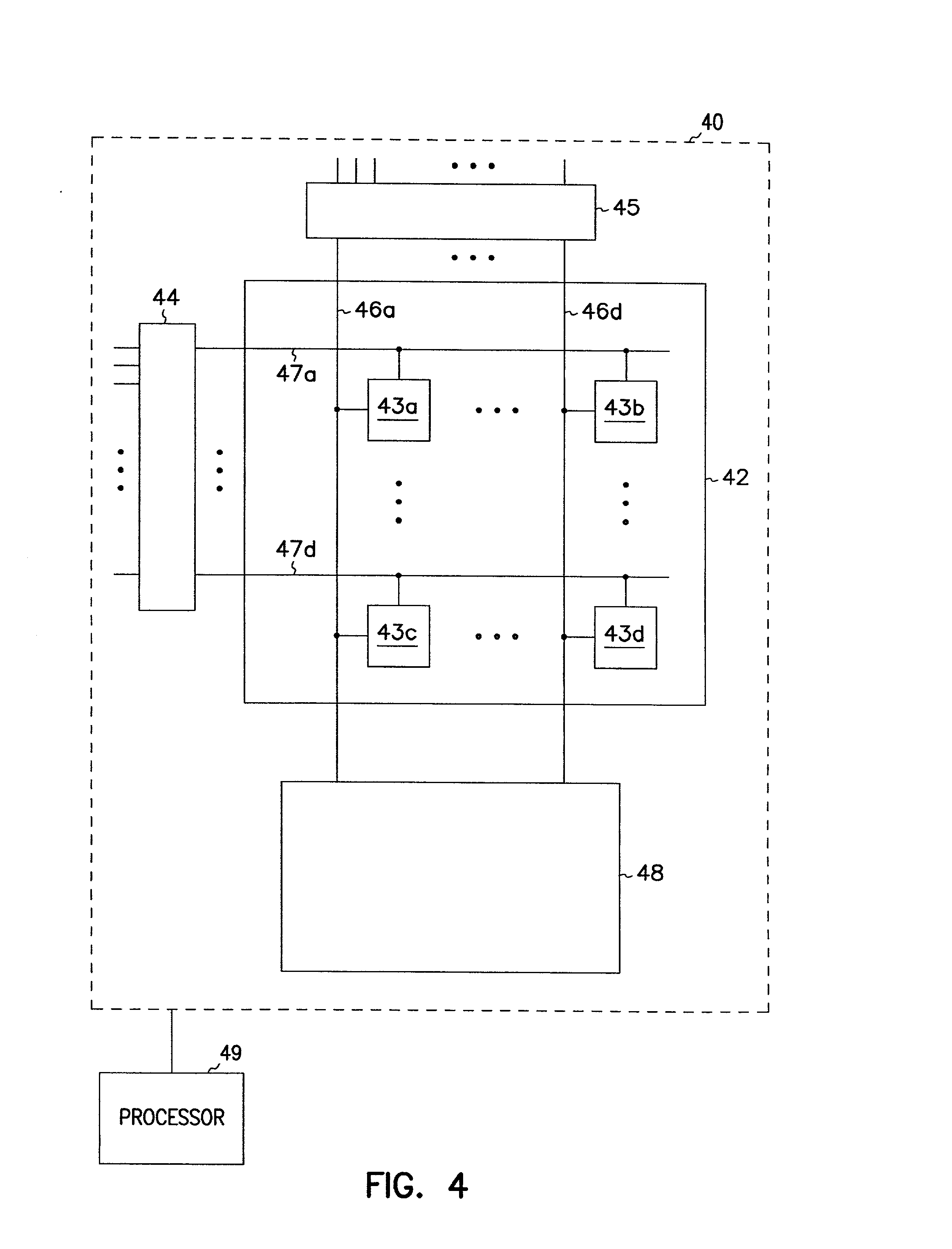
[0015] FIGS. 1-3 show a number of exemplary integrated-circuit assemblies, which taken collectively and sequentially, illustrate an exemplary method of fabricating a ferroelectric memory transistor according to the present invention. FIG. 4 shows an exemplary random-access-memory circuit incorporating ferroelectric memory transistors of the present invention. (As used herein, the term "ferroelectric," connotes any material or material structure, such as a layer, that exhibits a detectable spont...


PUM


Abstract

Integrated memory circuits, key components in thousands of electronic and computer products, have recently been made using ferroelectric memory transistors, which offer faster write cycles and lower power requirements than over conventional floating-gate transistors. One problem that hinders the continued down-scaling of conventional ferroelectric memory transistors is the vulnerability of their gate insulations to failure at thinner dimensions. Accordingly, the inventors devised unique ferroelectric gate structures, one of which includes a high-integrity silicon-oxide insulative layer, a doped titanium-oxide layer, a weak-ferroelectric layer, and a control gate. The doped titanium-oxide layer replaces a metal layer in the conventional ferroelectric gate structure, and the weak-ferroelectric layer replaces a conventional ferroelectric layer. These replacements reduce the permittivity mismatch found in conventional gate structures, and thus reduce stress on gate insulation layers, thereby improving reliability of ferroelectric memory transistors, particularly those with thinner gate insulation.

Description

RELATED APPLICATIONS[0001] This application is related to co-assigned application Ser. No. 09 / 383,726 (dockets 303.621US1, 99-0433) which was filed on Aug. 26, 1999 and to co-assigned application Ser. No. 09 / 594,817 (docket 99-1036) which was filed on Jun. 16, 2000. These applications are incorporated herein by reference.TECHNICAL FIELD[0002] The present invention concerns integrated memory circuits, ferroelectric memory transistors, and methods of making these circuits and transistors.BACKGROUND OF THE INVENTION[0003] Integrated memory circuits serve as data-storage components in thousands of products, from televisions, to automobiles, to computers. Typically, these memory circuits are implemented as arrays of floating-gate transistors, with each transistor storing an electrical charge representative of a one or a zero on its floating gate.[0004] In recent years, these floating-gate transistors have been modified to include a layer of ferroelectric material that exhibit electric po...

Claims


Application Information

Patent Timeline
IPC IPC(8): H01L21/28H01L27/115H01L29/51H01L29/78
CPCH01L21/28291H01L27/11502H01L29/516H01L29/78391H01L29/40111H10B53/00
Inventor AHN, KIE Y.FORBES, LEONARD
Owner MICRON TECH INC
Why Eureka
Try Eureka