LED array with optical isolation structure and method of manufacturing the same

an array and optical isolation technology, applied in the field of led arrays, can solve the problems of increasing the cost of led manufacturing, and increasing the time required for assembling each led into the precise position

Inactive Publication Date: 2002-10-24
INTEGRATED CRYSTAL TECH +2
View PDF0 Cites 45 Cited by
  • Summary
  • Abstract
  • Description
  • Claims
  • Application Information

AI Technical Summary

Problems solved by technology

However, when the LED apparatus becomes smaller, such as the LED array in a LED printer head or the LED array in a head mounted display, the size of each LED in the apparatus becomes very small therefore the packaging process becomes more complicated, see U.S. Pat. No. 5,014,074.
Therefore, the process of assembling each

Method used


Image

  • LED array with optical isolation structure and method of manufacturing the same
  • LED array with optical isolation structure and method of manufacturing the same
  • LED array with optical isolation structure and method of manufacturing the same

Examples


Embodiment Construction

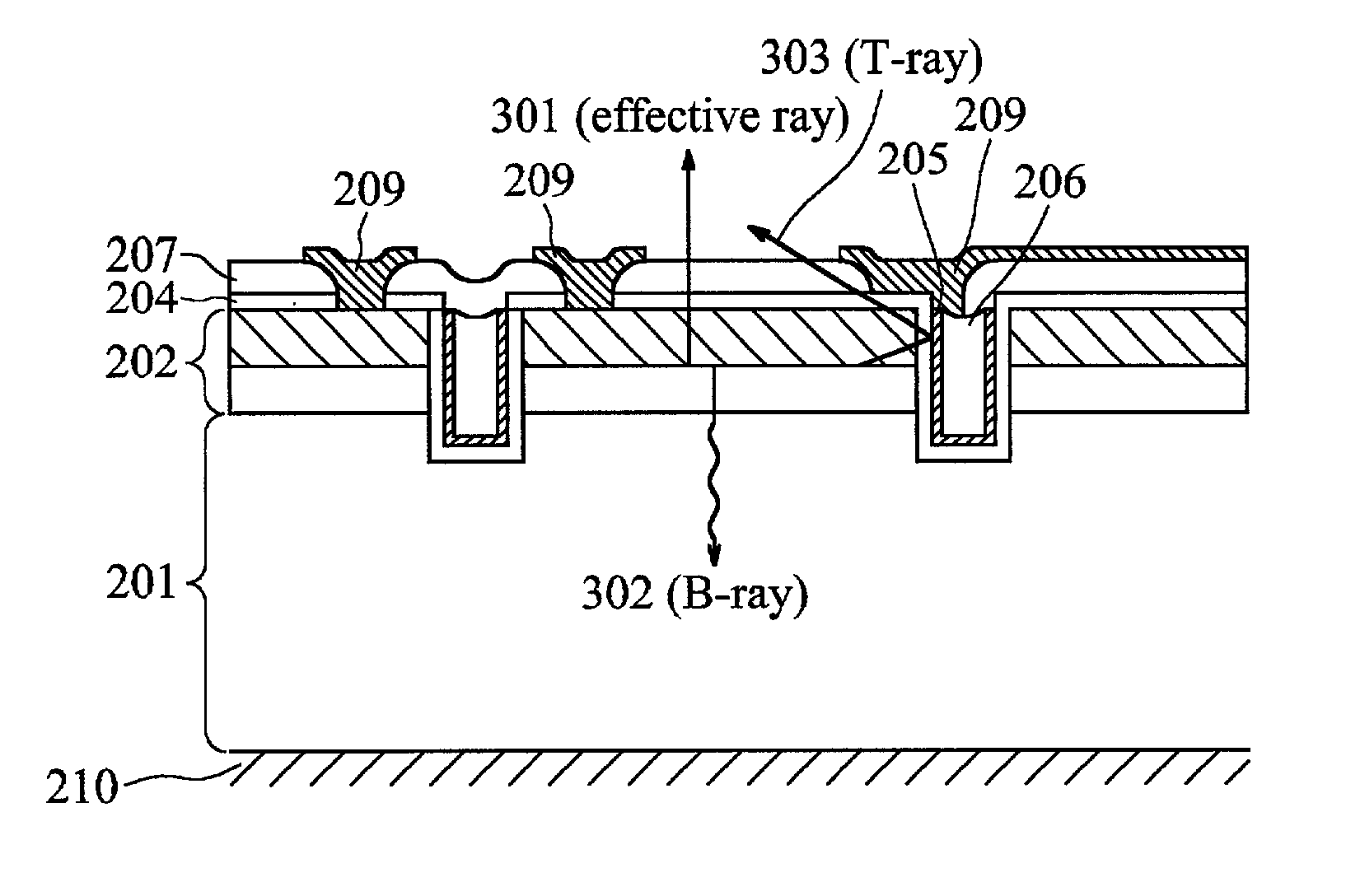
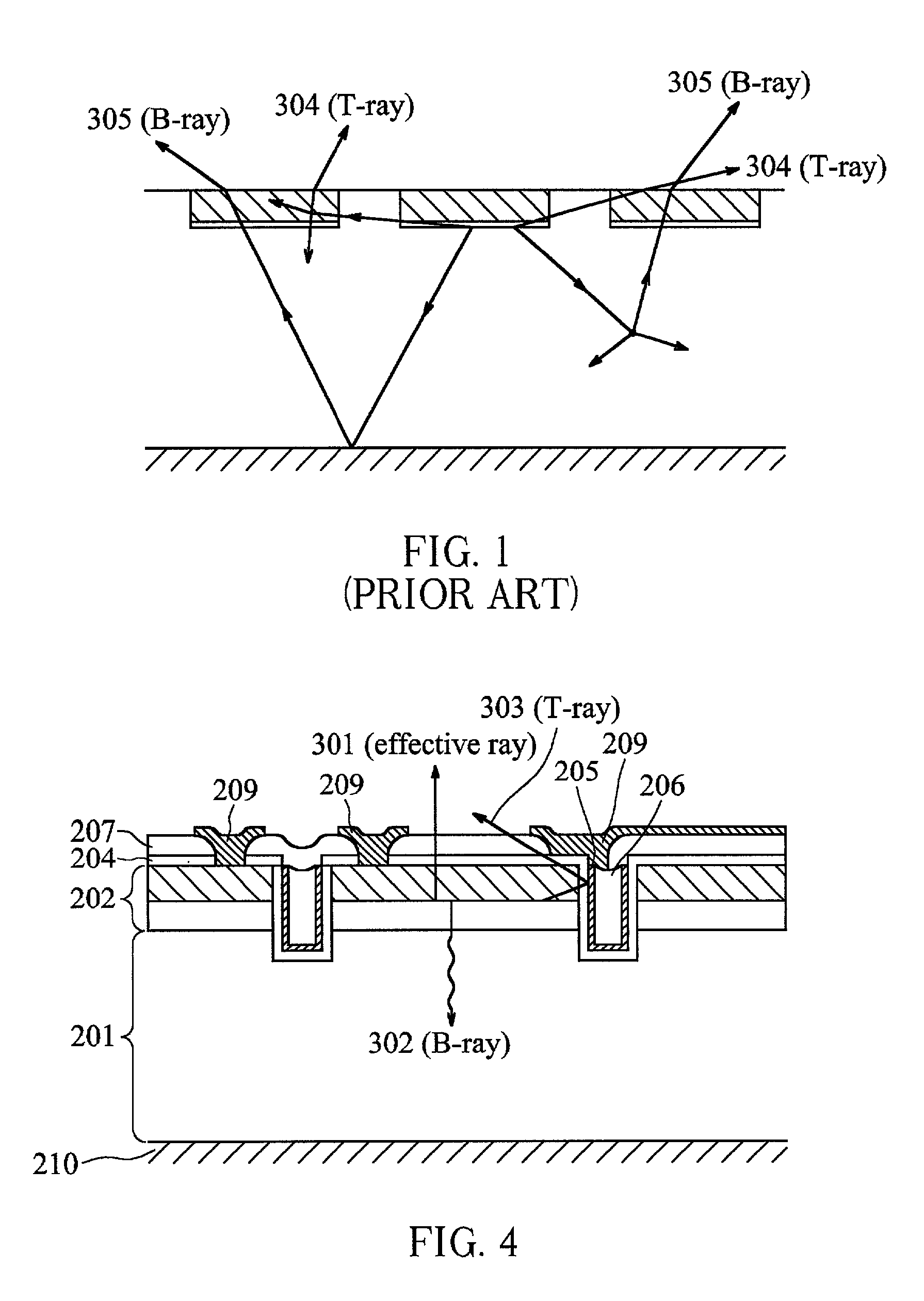
[0020] Referring to FIG. 1, the light transmitting routes and the cross-talk phenomenon in the traditional LED arrays are illustrated. As shown in FIG. 1, the lights emitted from a LED unit of the traditional LED array transmit into the surrounding LED units in two routes: One is called T-ray, which transferring in the transverse direction, transmitting through the boundary layer and emitting from the surface of the adjacent LEDs; and the other is called B-ray, which transferring downwardly to the base, transmitting through the substrate, reflected by the backside metal layer, and emitting from the surface of the adjacent LEDs. Thus, the light emitted from each LED is disturbed by T-rays and B-rays, and the image resolution of the LED array is decreased. This is called the cross-talk phenomenon in the traditional LED arrays, which can seriously damage the display resolution when high density array is designed.

[0021] Therefore, the present invention is to provide a LED array with an ...


PUM


Abstract

A Light Emitting Diode array (LED) with an optical isolation structure and a method of manufacturing the same. The LED array with an optical isolation structure includes a substrate, a plurality of LED units and a plurality of trenches. The plural LED units and trenches are disposed on the surface of the substrate. Each trench is disposed between every two LED units and deposited with at least one reflective metal layer. The substrate of the LED array with an optical isolation structure is formed of a low-energy-gap semiconductor material, while the LED units are formed by another kind of semiconductor material whose energy gap is higher than the substrate. The light emitted from each LED unit is reflected by the plural trenches deposited with at least one reflective metal layer, and absorbed by the substrate with low-energy gap.

Description

[0001] 1. Field of the Invention[0002] The present invention relates to an LED array for the LED display or the LED printer and the method of fabrication the same. Especially, the present invention is about an LED array with an optical isolation structure and a method fabricating thereof with a reduced cost.[0003] 2. Description of the Related Art[0004] Light emitting diodes (LEDs) have been widely used in many indicators, such as "ON / OFF" sign on the power switches. Nowadays, the brightness of LEDs has been greatly improved and the blue-light LED has been well developed. Besides, the LEDs are characterized by their extended long life, low energy consumption and low heat generation. Therefore, it becomes increasingly popular to utilize the light emitting diodes as illuminating sources, such as LED display panels or traffic light indicators etc.[0005] As described above, a plurality of LEDs can be arranged in a row or a matrix to construct a large-scale LED display or panel, such as ...

Claims


Application Information

Patent Timeline
IPC IPC(8): H01L27/15
CPCH01L27/156
Inventor SHIE, JIN-SHOWN
Owner INTEGRATED CRYSTAL TECH
Why Eureka
Try Eureka