

Optical module and optical communication system
a technology of optical communication system and optical module, which is applied in the field of optical modules, can solve the problems of large optical loss, high cost of welding method, and high thermal resistance of optical parts and adhesives, and achieve the effects of low cost, low cost, and reliable supply of conductivity
- Summary
- Abstract
- Description
- Claims
- Application Information
AI Technical Summary
Benefits of technology
Problems solved by technology
Method used
Image

Examples
first embodiment
[0066] A first embodiment concerns an optical module having an LD element and a PD element that monitors output of the LD element.
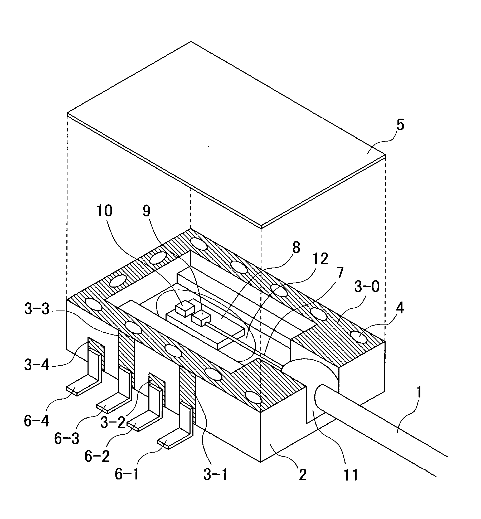
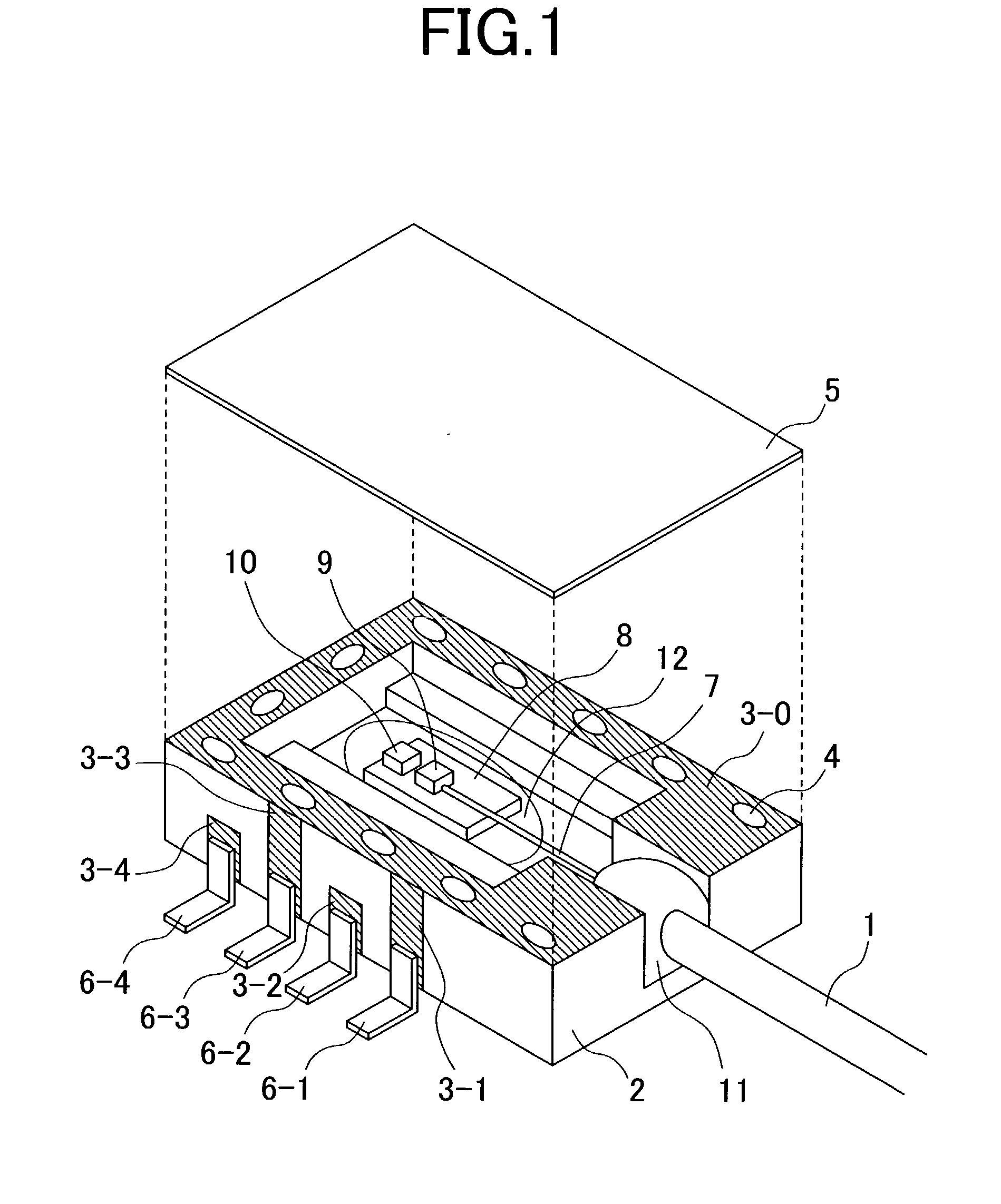
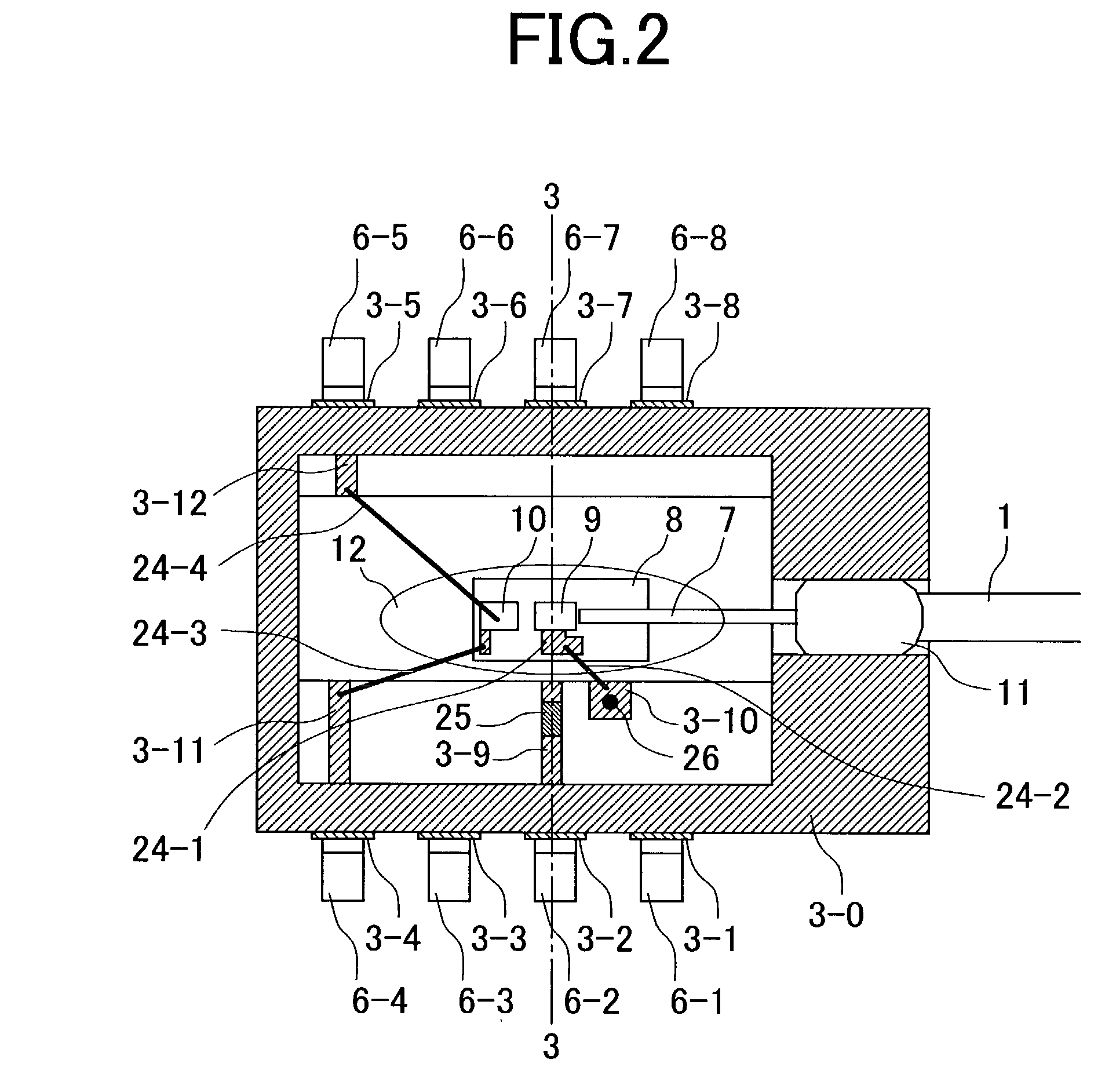
[0067] FIG. 1 is a perspective view of a LD module with a fiber pigtail according to the first embodiment of the present invention. In order to describe the inside of the LD module, and a method for bonding a cap, a cap 5 is shifted to a position above the LD module for the sake of illustration. Here, a part of details on an internal electrode pattern, a wire bond, and the like, are omitted. FIG. 2 is a plan view illustrating a state before the cap of the LD module shown in FIG. 1 is mounted. In FIG. 2, the electrode patterns, the wire bonds, and the like, inside the module are also illustrated in detail. FIG. 3 is a cross section of the LD module taking along line 3-3 in FIG. 2. A main body of the ceramic package is formed of three ceramic lamination layers. FIGS. 4 to 7 illustrate respective electrode patterns of three ceramic plate layers, which consti...
second embodiment
[0077] A second embodiment is an optical module having a PD element and an IC element which amplifies output of the PD element.
[0078] FIG. 8 is a perspective view of a PD module with a fiber pigtail according to the second embodiment of the present invention. In order to describe the inside of the PD module, and a method for bonding a cap, the cap 5 is shifted to a position above the PD module for the sake of illustration. Here, a part of details on an electrode pattern, wire bonds, and the like, inside the package are omitted. FIG. 9 is a plan view of the PD module in FIG. 8, illustrating a state before the cap of the PD module is mounted. In FIG. 9, the electrode pattern, the wire bonds, and the like, inside the package are also illustrated in detail. FIG. 10 is a cross section of the PD module taken along line 10-10 in FIG. 9. FIGS. 11 to 14 illustrate respective electrode patterns of three ceramic plate layers, which constitute a ceramic package main body 4 of the PD module. FIG...
fourth embodiment
[0093] A fourth embodiment is characterized by a devised shape of a cap.
[0094] FIG. 16 is a perspective view of a PD module with a fiber pigtail according to the fourth embodiment of the present invention. In order to describe the inside of the module and a method for securing a metal cap 5, the metal cap 5 is shifted to a position above the module for the sake of illustration. In a state in which the present invention is actually embodied, the cap 5 is secured to an electrode pattern on the bottom of a main body 2 using a conductive adhesive 4.
[0095] Although this PD module has the same function as the PD module shown in the second embodiment, this module is different from that of the second embodiment in the following points:
[0096] (1) The metal cap is bent in such a manner as to extend to a part of the back of the main body.
[0097] (2) There is not the electrode pattern 3-0 on the top surface of the package as shown in FIG. 8. The metal cap 5 is electrically connected to a ground ...
PUM
 Abstract
Description
Claims
Application Information