Semiconductor device with elongated interconnecting member and fabrication method thereof

Inactive Publication Date: 2002-12-12
LAPIS SEMICON CO LTD
View PDF0 Cites 11 Cited by
  • Summary
  • Abstract
  • Description
  • Claims
  • Application Information

AI Technical Summary

Problems solved by technology

As a result, it has become difficult to assure the stable formation of a resist pattern for the small-diameter through holes in the photolithographic process, and to assure that the through holes will be etched to a constant depth during the etching process.
The result is unreliable connections between the different wiring layers of a semiconductor device with mu

Method used


Image

  • Semiconductor device with elongated interconnecting member and fabrication method thereof
  • Semiconductor device with elongated interconnecting member and fabrication method thereof
  • Semiconductor device with elongated interconnecting member and fabrication method thereof

Examples


first embodiment

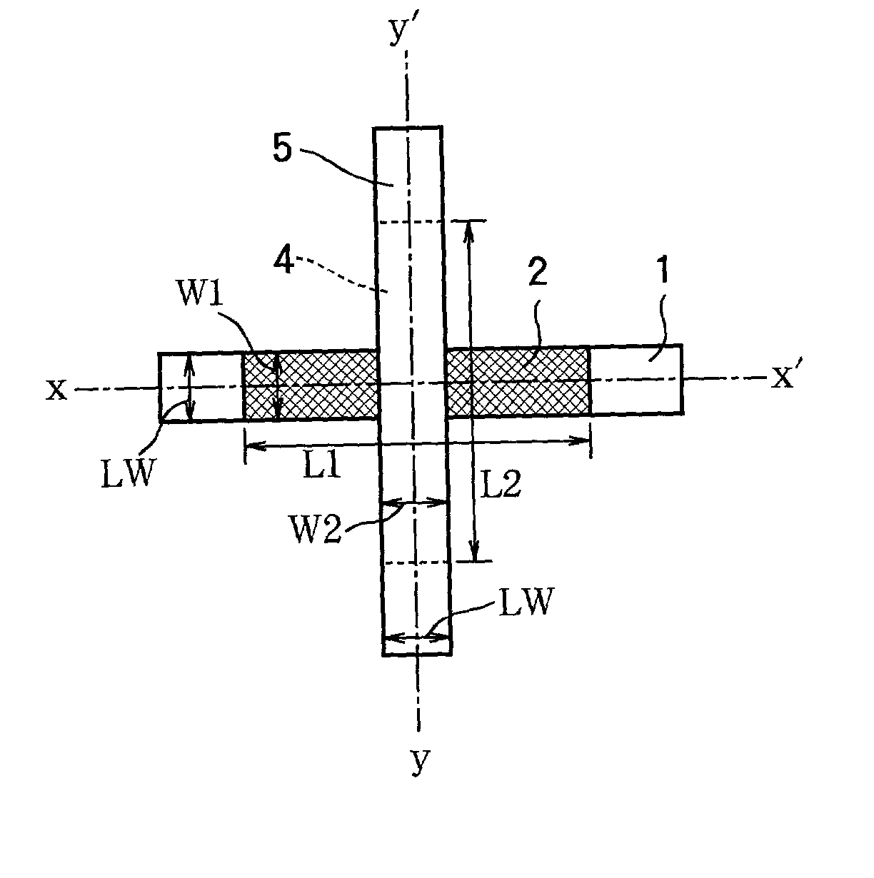
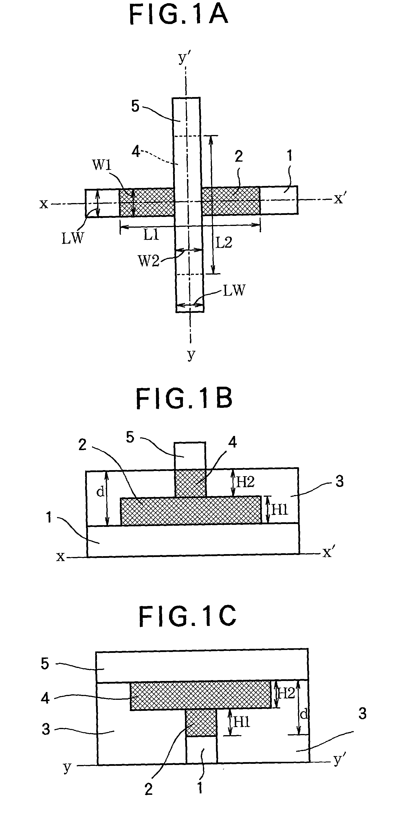
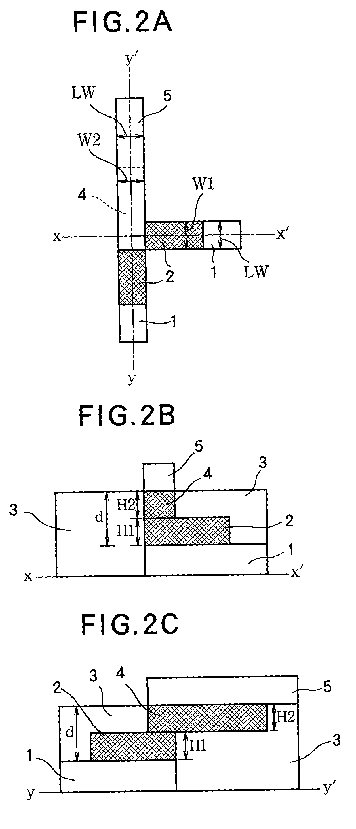
[0052] The structure of a semiconductor device is illustrated in FIGS. 1A to 4C. As shown in these drawings, the semiconductor device includes a first conductive line or first conductive pattern 1 in a lower conductive layer, a first conductive member or first conductor in the form of a rectangular metal bar 2, an inter-layer dielectric film 3, a second conductive member or second conductor in the form of a rectangular metal bar 4, and a second conductive line or second conductive pattern 5 in an upper conductive layer. Both conductive lines (or patterns) 1, 5 have a line width LW, rectangular metal bar 2 has height H1, and rectangular metal bar 4 has height H2. The separation d between the upper conductive layer and the lower conductive layer is the sum of heights H1 and H2.

[0053] In each drawing, rectangular metal bar 2 is aligned above and in contact with lower-layer conductive line 1, while rectangular metal bar 4 is aligned below and in contact with upper-layer conductive line...

second embodiment

[0119] FIGS. 10A to 10C and 11A to 11C show the structure of a semiconductor device according to a second embodiment of the present invention. FIGS. 10A and 11A are partial plan views of the device, FIGS. 10B and 11B are sectional views through line x-x' in FIGS. 10A and 11A, respectively, and FIGS. 10C and 11C are sectional views through line y-y' in FIGS. 10A and 11A, respectively. As shown in these drawings, the semiconductor device includes a conductive line 31 in a lower conductive layer, a first conductive member in the form of a rectangular metal bar 32, an inter-layer dielectric film 33, a second conductive member in the form of a rectangular metal bar 34, and a conductive line 35 in an upper conductive layer. The rectangular metal bar 32 has a height h1, the rectangular metal bar 34 has a height h2, and the lower-layer conductive line 1 and upper-layer conductive line 5 are mutually separated by a distance d. In the interconnection structure in FIGS. 10A to 10C, the two con...

third embodiment

[0127] FIGS. 12A to 12c show the structure of a semiconductor device according to a third embodiment of the invention. FIG. 12A is a partial plan view, FIG. 12B is a sectional view through line x-x' in FIG. 12A, and FIG. 12C is a sectional view through line y-y' in FIG. 12A. As shown in these drawings, the semiconductor device includes a conductive line 41 in a lower conductive layer, a conductive member in the form of a rectangular metal bar 42, an inter-layer dielectric film 43, a through hole 44, and a conductive line 45 it an upper conductive layer. Rectangular metal bar 42 has a height H1; the through hole 44 has a depth D2 and diameter r2. A separation d is provided between the lower-layer conductive line 41 and the upper-layer conductive line 45. In FIGS. 12A to 12c, the lower-layer conductive line 41 bends at substantially at a right angle and the upper-layer conductive line 45 terminates above the bend in the lower-layer conductive line 41; the end of the upper-layer conduc...


PUM


Abstract

In a semiconductor device with multiple wiring layers, to connect a conductive line in a lower wiring layer to a conductive line in an upper wiring layer, two conductive members are formed in the space between the upper and lower conductive layers, one conductive member in contact with each conductive line. The two conductive members meet in the space between the two conductive layers to form an electrical path between the two conductive lines. One or both of the conductive members may have a rectangular bar shape extending lengthwise along the conductive line with which it makes contact. The conductive members can have a reduced height and enlarged area that enables interconnections to be formed with greater stability and reliability than by conventional methods.

Description

[0001] 1. Field of the Invention[0002] The present invention relates to a semiconductor device having multilayer wiring, and more particularly to a method of forming interconnections between an upper wiring layer and a lower wiring layer.[0003] 2. Description of the Related Art[0004] FIG. 14 shows a partial sectional view of a conventional semiconductor device having a lower conductive layer or wiring layer including a first conductive line or wire 61, an inter-layer dielectric film 62 with a through hole 63, and an upper conductive layer or wiring layer including a second conductive line or wire 64 that is connected to the lower-layer wire 61 by a metal plug filling the through hole 63. The through hole 63 has a depth d, radius r, and diameter 2r.[0005] The multilayer wiring structure shown in FIG. 14 is fabricated as follows. First, a layer of metal is deposited on the entire surface of the device and patterned by photolithography and etching to form a lower-layer pattern of condu...

Claims


Application Information

Patent Timeline
IPC IPC(8): H01L21/768H01L23/522
CPCH01L21/76838H01L23/5226H01L2924/0002H01L2924/00H01L23/5283
Inventor TANAKA, HIROYUKI
Owner LAPIS SEMICON CO LTD
Why Eureka
Try Eureka