

Production method of suspension board with circuit
a production method and suspension board technology, applied in the direction of record information storage, resistive material coating, maintaining head carrier alignment, etc., can solve problems such as unstable plating and product defects, and achieve the effect of preventing erosion, preventing deterioration of the outward appearance and defects of products
- Summary
- Abstract
- Description
- Claims
- Application Information
AI Technical Summary
Benefits of technology
Problems solved by technology
Method used
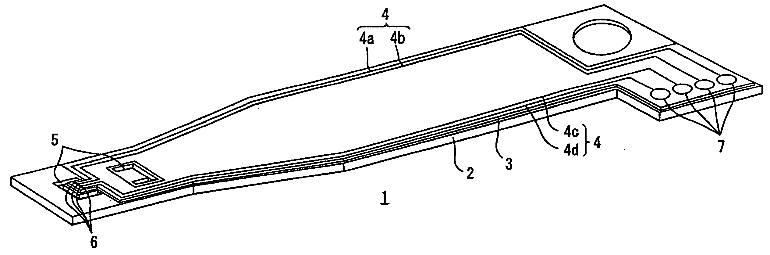
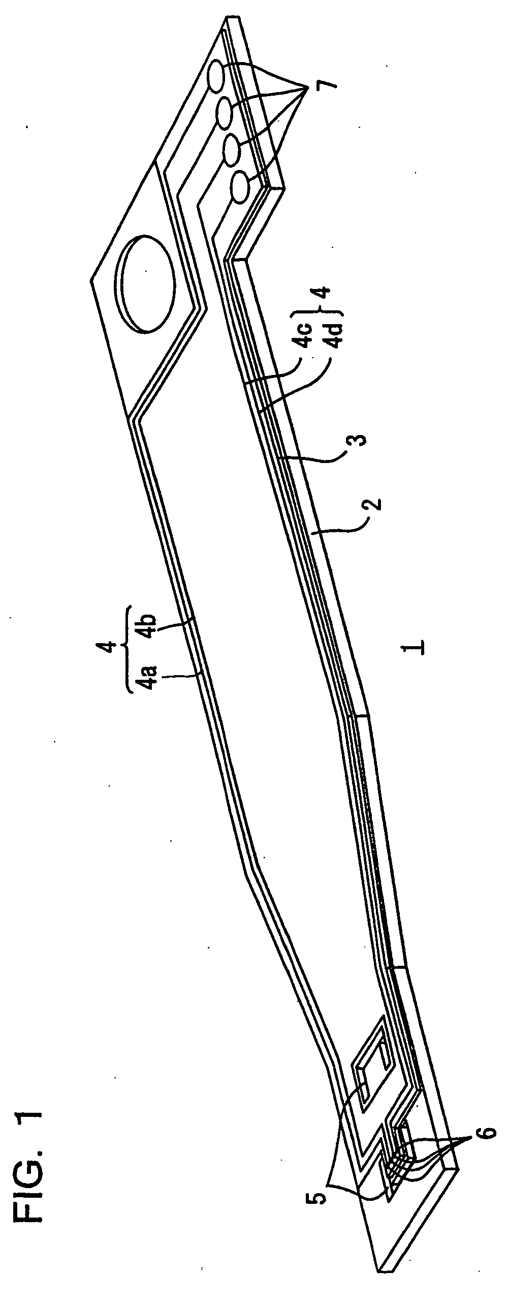
Image

Examples
example
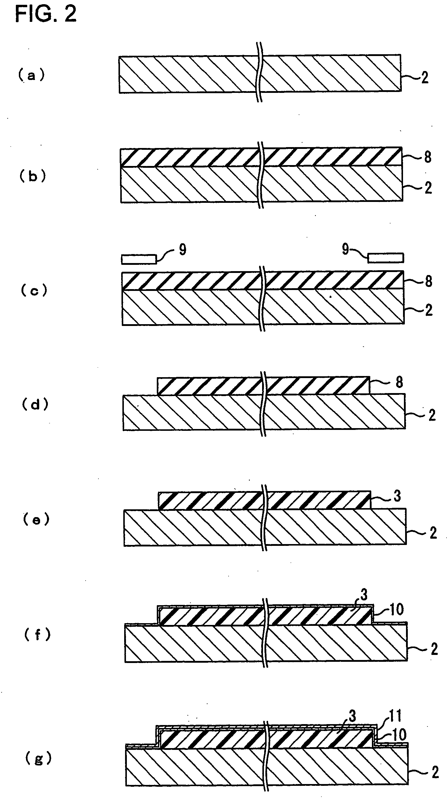
[0084] The invention will now be described more concretely in an example described below. It should be appreciated, however, that the invention is not particularly limited to the example below.
[0085] A stainless (SUS304) foil having a thickness of 25 μm was prepared (Cf. FIG. 2(a)).
[0086] Meanwhile, a solution of precursor of a photosensitive polyimide resin was prepared in the following manner. That is, 0.702 kg (6.5 moles) of p-phenylene diamine, 1.624 kg (5.5 moles) of 3,4,3′,4′-biphenyltetracarboxylic dianhydride (diphthalic dianhydride), and 0.444 kg (1.0 mole) of 2,2-bis(3,4-dicarboxy-phenyl)hexafluoropropane (6FDA) (a total of acid anhydrides: 6.5 kg) were dissolved in 19.72 kg of dimethyl acetamide, and kept stirred for 72 hours at room temperature.
[0087] Subsequently, the resulting solution was heated to 75° C., and the heating was stopped when the viscosity reached 5000 centipoises (5 Pa·s). The solution was then let stand until it was cooled to room temperature. Then, ...
PUM
| Property | Measurement | Unit |
|---|---|---|
| width | aaaaa | aaaaa |
| width | aaaaa | aaaaa |
| width | aaaaa | aaaaa |
Abstract
Description
Claims
Application Information