
III nitride compound semiconductor device

a technology of nitride and semiconductors, applied in the direction of semiconductor devices, thermoelectric device junction materials, electrical apparatus, etc., can solve the problems of bringing about the aforementioned various problems

Inactive Publication Date: 2003-02-06
TOYODA GOSEI CO LTD
View PDF13 Cites 34 Cited by
  • Summary
  • Abstract
  • Description
  • Claims
  • Application Information

AI Technical Summary

Benefits of technology

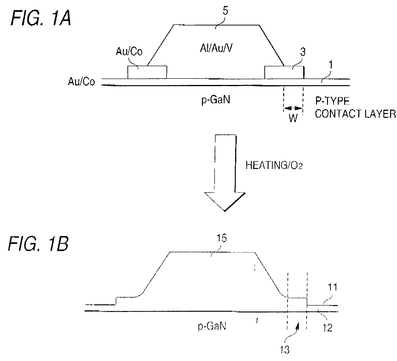
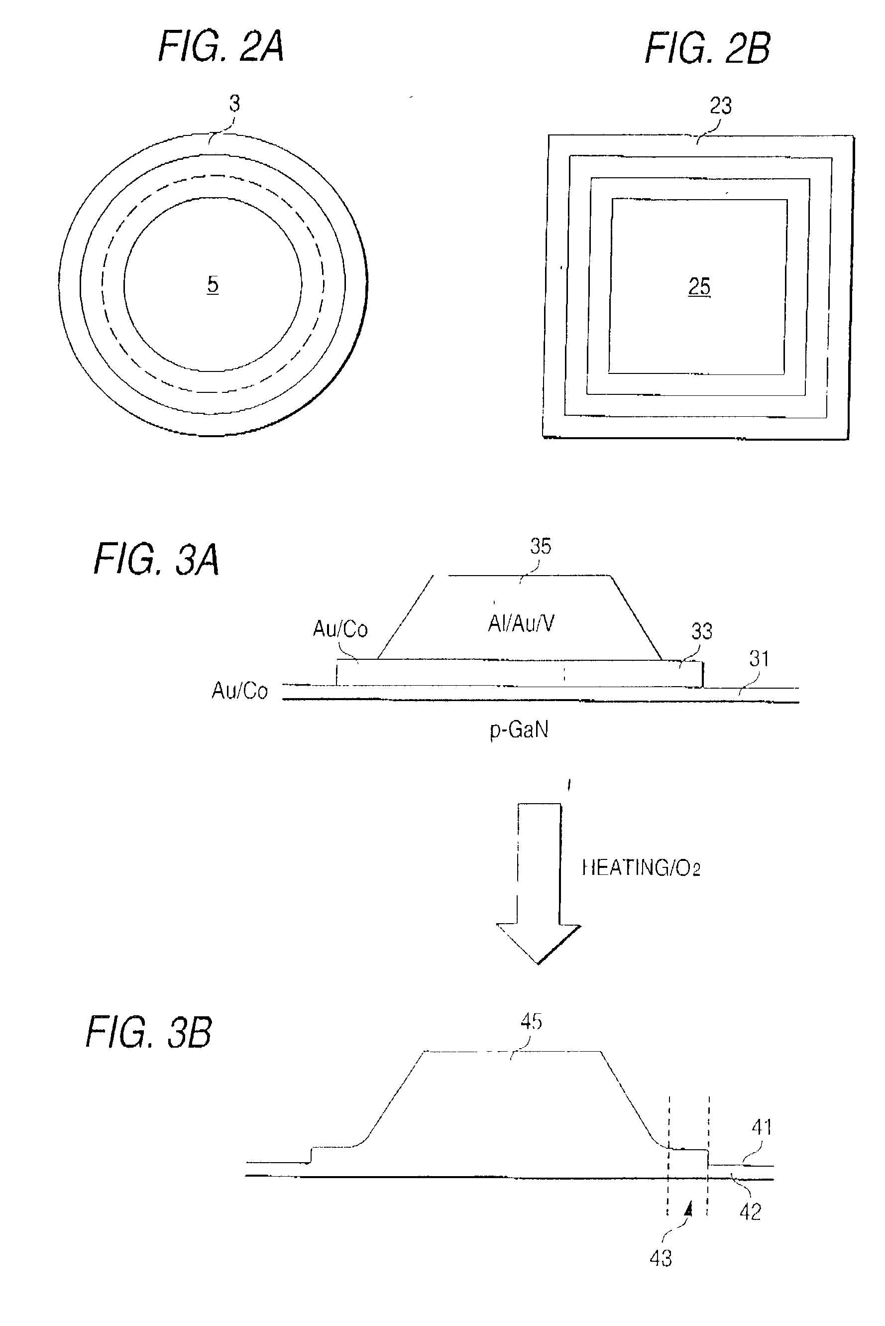
0009] According to the Group III nitride compound semiconductor device configured in this manner, the portion of the translucent electrode coming in contact with the circumferential surface of the p-type pad electrode is made thick, so that the area of a joint surface between the translucent electrode and the circumferential surface of the pad electrode is increased, compared with the translucent electrode having no thick portion. Because it is inferred that the allowable current is proportional to the area of the joint surface between the translucent electrode and the circumferential surface of the pad electrode, the current allowed to be applied to the pad electrode is increased in the device according to the present invention in which the thick portion is provided.
0010] In addition, because adhesion (mechanical strength) between the translucent electrode and the circumferential surface of the pad electrode is strengthened by the presence of the thick portion, any crack hardly occurs between the two. Also from this point of view, the allowable current is prevented from being limited.

Problems solved by technology

As a result, the area of contact between the two is reduced to thereby bring about the aforementioned various problems.

Method used


Image

  • III nitride compound semiconductor device
  • III nitride compound semiconductor device
  • III nitride compound semiconductor device

Examples


Embodiment Construction

[0028] Members of the invention will be described below in detail.

[0029] As shown in FIG. 1B, a translucent electrode 11 has a thick portion 13 connected to a circumferential surface of a pad electrode 15, and a thin portion 12 as the remainder.

[0030] The thickness and material of the thin portion 12 are not particularly limited but it is preferable that the thin portion 12 is made of a translucent material such as a gold alloy and is made as thin as possible from the point of view of transmitting light in the case of a light-emitting device. For example, in the case of a gold alloy, the thickness of the thin portion 12 is preferably set to be in a range of from 4 to 40 nm, more preferably in a range of from 4 to 30 nm, further preferably in a range of from 4 to 15 nm, most preferably in a range of front 4 to 10 nm.

[0031] The thickness of a thickest portion (a portion joined to the pad electrode 15) of the thick portion 13 is preferably set to be in a range of from 1.5 times to 15 t...


PUM

PropertyMeasurementUnit
thicknessaaaaaaaaaa
widthaaaaaaaaaa
thicknessaaaaaaaaaa

Abstract

The present invention provides a Group III nitride compound semiconductor device in which the amount of a current allowed to be applied on a p-type pad electrode can be increased. That is, in the Group III nitride compound semiconductor device according to the present invention, a portion of a translucent electrode coming in contact with a circumferential surface of the p-type pad electrode is formed as a thick port ion to thereby increase the area of contact between the circumferential surface and the translucent electrode to thereby increase the current allowed to be applied on the p-type pad electrode. In addition, the use of the thick portion prevents cracking from occuring between the translucent electrode and the circumferential surface of the pad electrode.

Description

[0001] The present invention relates to a Group III nitride compound semiconductor device. More specifically, it relates to improvement in a p-type translucent electrode of a Group III nitride compound semiconductor device.[0002] In a Group III nitride compound semiconductor light-emitting device such as a blue light-emitting diode, especially, in a light-emitting device having a substrate disposed on a lower side, a thin translucent electrode is formed on an almost whole surface of a p-type contact layer having relatively large resistance in order to distribute a current into the p-type contact layer evenly to thereby obtain uniform light emission form the whole area of a light-emitting layer. Because wire-bonding cannot be applied directly to such a thin translucent electrode, a pad electrode is formed thereon (see Japanese Unexamined Patent Publication No. JP-A-H09-320984, and so on).[0003] The present inventors have made an examination of further reduction in thickness of the tr...

Claims


Application Information

Patent Timeline
Patent Type & Authority Applications(United States)
IPC IPC(8): H01L21/28H01L21/205H01L29/20H01L29/43H01L29/45H01L33/32H01L33/38H01L33/42H01L33/62
CPCH01L29/2003H01L29/452H01L33/32H01L33/38H01L33/40
Inventor UEMURA, TOSHIYAHIRANO, ATSUOHORIUCHI, SHIGEMI
Owner TOYODA GOSEI CO LTD
Learn More