
Method and apparatus for detecting a wafer's posture on a susceptor

a susceptor and semiconductor technology, applied in the direction of crystal growth process, optical radiation measurement, instruments, etc., can solve the problems of deteriorating uniform thickness and quality of thin silicon layer deposited on the surface of the wafer, and the robot may not correctly position the wafer 1 within a step formed,

Inactive Publication Date: 2003-03-06
TOSHIBA MASCH CO LTD
View PDF0 Cites 384 Cited by
  • Summary
  • Abstract
  • Description
  • Claims
  • Application Information

AI Technical Summary

Benefits of technology

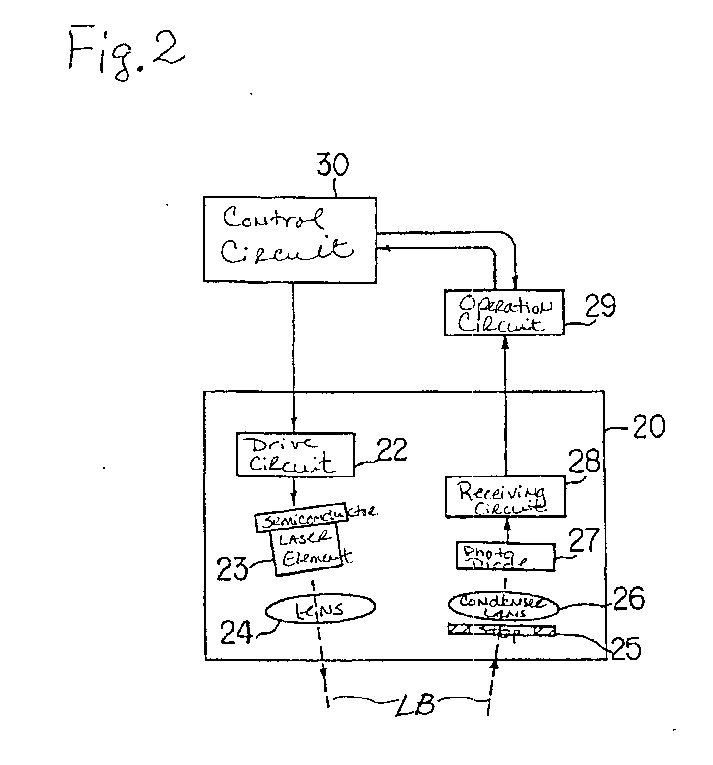
[0022] The stop mechanism including an adjustable aperture may be located in front of the photo sensitive detector. The stop mechanism may be used to limit the quantity of an incident laser beam focused at the receiving area may be limited. In such an arrangement, it is possible to close the aperture so that no incident laser beam reaches the receiving area when the wafer's slope exceeds a predetermined degree. Therefore, the stop mechanism increases the accuracy of determining the wafer's posture or slope.

Problems solved by technology

Nevertheless, the conventional devices suffer from several disadvantages.
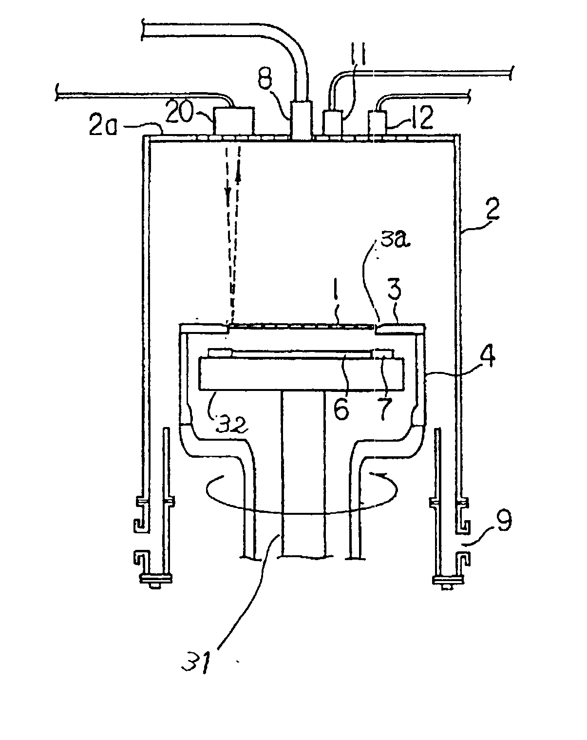
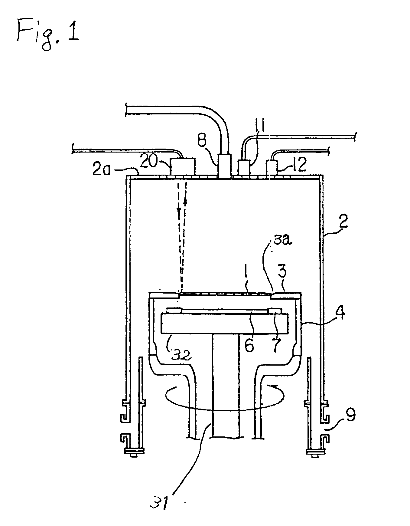
However, because an error may develop within the position control mechanism of the robot's hand or fork, the robot may not correctly position the wafer 1 within a step formed on the upper, inside surface of the ring of the susceptor 3.
As the result, the uniform thickness and the quality of the thin silicon layer deposited on the wafer's surface deteriorates.
Furthermore, when the device rotates a misaligned wafer, the wafer 1 may become dislodged from the susceptor 3 as the rotational speed increases causing damage to the wafer 1 and to the components of and the interior surface of the reaction chambers.

Method used


Image

  • Method and apparatus for detecting a wafer's posture on a susceptor
  • Method and apparatus for detecting a wafer's posture on a susceptor
  • Method and apparatus for detecting a wafer's posture on a susceptor

Examples


Embodiment Construction

[0030] The embodiment according to the invention will be explained below with reference to the attached drawings.

[0031] FIG. 1 shows an epitaxial vapor growing device on which an apparatus for detecting the posture of a wafer positioned on a susceptor. FIG. 1 illustrates a detection head 20 for a wafer posture which includes a source for emitting a laser beam and a detector for receiving the reflected laser beam. The detection head 20 mounts onto the ceiling 2a of a reaction chamber 2, and the detection head 20 directs its laser beam through a window mounted on ceiling 2a to the circumference of the wafer 1.

[0032] FIG. 2 shows an outline of the apparatus for detecting the wafer's posture according to this embodiment. In FIG. 2, the detection head 20 contains a drive circuit 22, an semiconductor laser element 23 for generating a laser, a len 24 for irradiating a laser beam, a stop mechanism 25, condenser lens 26, a photo diode 27 and a receiving circuit 28.

[0033] In response to an in...


PUM


Abstract

An apparatus used for an epitaxial vapor growing arrangement and for detecting whether a wafer is properly seated within a susceptor contained therein. The apparatus includes a semiconductor laser element that generates a laser beam which irradiates the wafer's surface. The apparatus, further, includes a combination of a stop mechanism, a condenser lens and a photo diode, which detects the laser beam reflected from the wafer surface and an operation circuit, which determines the wafer's posture on the susceptor. During operation, the reflected laser beam focuses on a receiving surface of the photo diode through the condenser lens. The operation circuit then compares the output signal from the photo diode with a preset reference value for discriminating the slope of the wafer.

Description

[0001] 1. Field of the Invention[0002] This invention relates to an epitaxial vapor growing device for manufacturing semiconductor waters, and more particularly, to an apparatus for detecting and adjusting the position of a semiconductor wafer positioned on a susceptor within the epitaxial vapor growing device.[0003] 2. Description of Related Art[0004] FIG. 5 shows a conventional epitaxial vapor growing device typically used to manufacturing semiconductor wafers by depositing a thin layer of silicon onto the surface of the wafer.[0005] In FIG. 5, a reaction chamber 2 includes a susceptor 3, located approximately in the center of the reaction chamber, to support a wafer 1 thereon. The shape of the susceptor 3 may resemble a ring, which is fixedly mounted on a hollow bearer 4 and connected to a motor drive unit (not shown) so as to rotate the susceptor 3.[0006] The hollow bearer 4 includes a fixed column 31 supporting a table 32. Mounted onto the table 32 are a disc like heater 6 and ...

Claims


Application Information

Patent Timeline
IPC IPC(8): H01L21/68C30B25/16G01B11/03H01L21/00
CPCC30B25/16H01L21/67265
Inventor KATSUMATA, HIROHUMIKOBAYASHI, TAKEHIKO
Owner TOSHIBA MASCH CO LTD
Learn More