Thermoelectric device and optical module made with the device and method for producing them

a technology of thermoelectric devices and optical modules, which is applied in the manufacture/treatment of thermoelectric devices, semiconductor devices, and semiconductor devices. it can solve the problems of difficult to obtain a size less than 500 .mu.m, insufficient limitation of thermoelectric devices a in reducing the size, and material allowed

Inactive Publication Date: 2003-03-27
SUMITOMO ELECTRIC IND LTD +2
View PDF0 Cites 41 Cited by
  • Summary
  • Abstract
  • Description
  • Claims
  • Application Information

AI Technical Summary

Problems solved by technology

Thermoelectric device A has an insufficient limitation in reducing the size of the thermoelectric element because the thermoelectric element is processed one by one.
At present, it is difficult to obtain a size less than 500 .mu.m.
This method has a limitation in that only one type of material is allowed to produce the columnar structure.
As a result, a thermoelectric device having a structure in which thermoelectric elements are sandwiched between two ceramic substrates becomes large, thereby making the heat-flow design difficult.
However, it is difficult to decrease the size of the thermoelectric element in the X and Y directions to less than 500 .mu.m with the structure of the above-described conventional Thermoelectric device A. On the other hand, the thermoelectric element can be miniaturized with the structure of the conventional Th...

Method used


Image

  • Thermoelectric device and optical module made with the device and method for producing them
  • Thermoelectric device and optical module made with the device and method for producing them
  • Thermoelectric device and optical module made with the device and method for producing them

Examples


Embodiment Construction

(1) Production of Mold for Forming Thermoelectric Elements

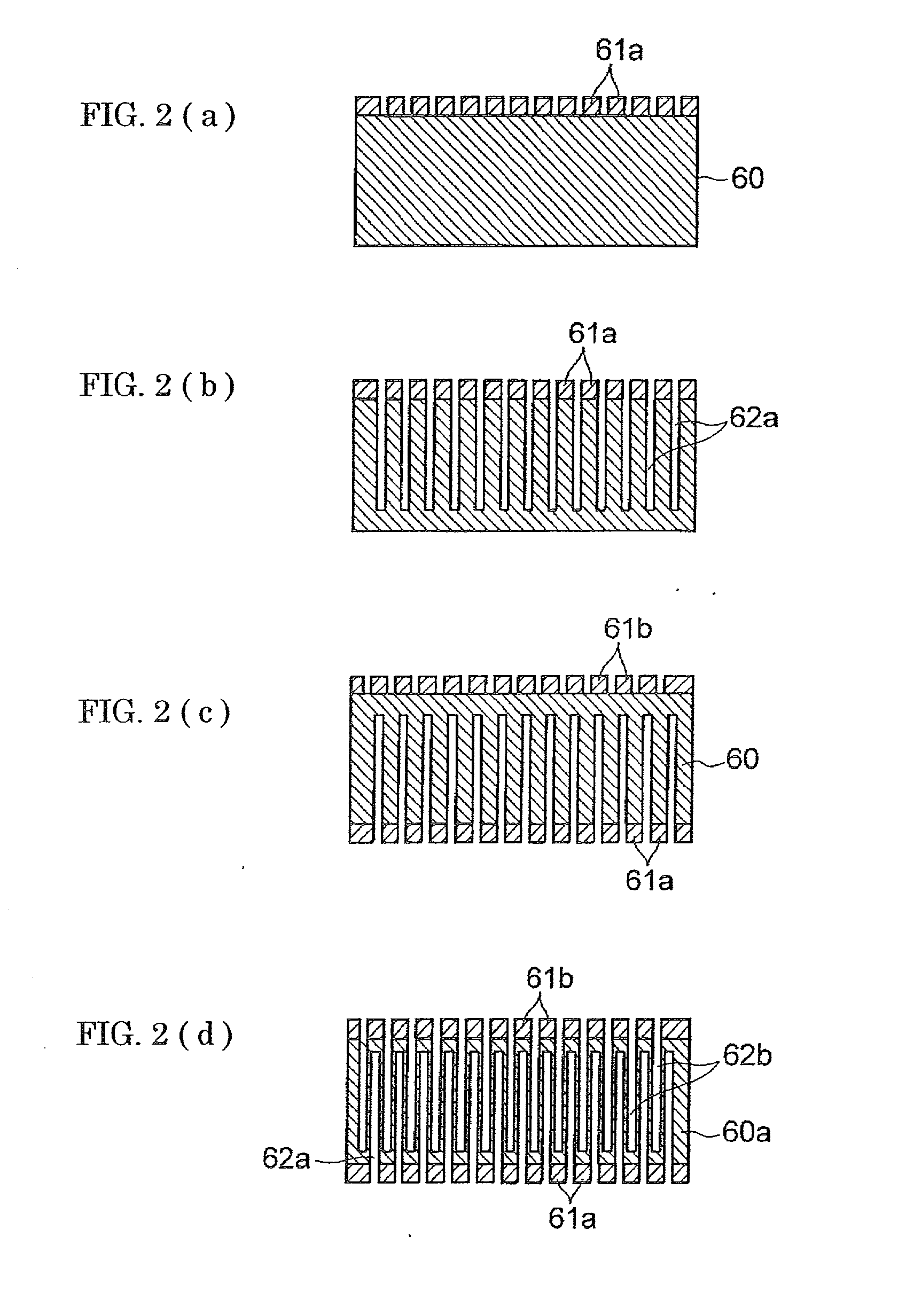
[0105] As shown in FIG. 2(a), an Si wafer having a thickness of 600 .mu.m was prepared as a base material 60. A photoresist pattern 61a made of an organic substance was formed on the front side of the Si wafer by photolithography. Small holes formed in the photoresist 61a had the shape of a square. As shown in FIG. 2(b), only the front side of the base material 60 was treated by reactive-ion etching using SF.sub.6 as an Si-reactive ion gas and C.sub.4F.sub.8 as a protective gas for the walls of the small holes. This treatment formed quadrangular prism-shaped small holes 62a, each having a square cross section with a side length of 40 .mu.m and a depth of 500 .mu.m, regularly arranged in the X and Y directions with a pitch of 120 .mu.m.

[0106] A gas to be used for the reactive-ion etching of the base material has only to be capable of etching it. In the case of an Si base material, not only SF.sub.6 but also other reactive ion ...


PUM


Abstract

A thermoelectric device that realizes miniaturization and densification, an optical module incorporating the thermoelectric device, and their production method. N-type thermoelectric elements 51 and p-type thermoelectric elements 52 are arranged orthogonally and alternately, on the XY-plane, in a matrix consisting of at least four elements in total in a row and at least four elements in total in a column. All the thermoelectric elements 51 and 52 have a size of at most 250 mum in the X and Y directions. At most four thermoelectric elements nearest to an n-type thermoelectric element 51 are of p type, and at most four thermoelectric elements nearest to a p-type thermoelectric element 52 are of n type. The thermoelectric elements 51 and 52 are bonded through metallic bonding materials to electrodes 53 having the shape of a rectangle or a rounded rectangle formed on an insulating substrate 54.

Description

[0001] 1. Field of the Invention[0002] The present invention relates to (a) a thermoelectric device used for thermal power generation, which converts thermal energy into electric power, and electronic cooling through the Peltier effect and (b) an optical module for optical communication incorporating the thermoelectric device.[0003] 2. Description of the Background Art[0004] Thermoelectric devices are used for generating power by using the otherwise useless heat generated in a computer or an automobile and as a device for cooling ICs in a computer or laser-diodes (LDs) for optical communication. Such thermoelectric devices are produced by coupling a multitude of n-type and p-type thermoelectric elements through electrodes made of, for example, metal. Their structures are broadly classified into two types.[0005] One type is represented by a thermoelectric device described in the published Japanese utility-model application Jitsukaishou 59-91765, for example. This type is referred to ...

Claims


Application Information

Patent Timeline
IPC IPC(8): H01L35/32H01L35/34
CPCH01L35/32H01L35/34H10N10/01H10N10/17
Inventor TATOH, NOBUYOSHILI, JING-FENGWATANABE, RYUZOTANAKA, SHUJIESASHI, MASAYOSHI
Owner SUMITOMO ELECTRIC IND LTD
Why Eureka
Try Eureka