
Imaging optical system and exposure apparatus

an optical system and exposure apparatus technology, applied in the direction of photomechanical apparatus, instruments, printers, etc., can solve the problems of difficult illumination system design, no na on the order, and difficult beam isolation

Inactive Publication Date: 2003-04-24
NIKON CORP
View PDF2 Cites 58 Cited by
  • Summary
  • Abstract
  • Description
  • Claims
  • Application Information

AI Technical Summary

Problems solved by technology

Because there are no materials having transmittances that would allow adequate formation of an optical system from refractive elements at this range of wavelengths, such optical systems must be constructed exclusively from reflective surfaces.
And yet, of the many EUVL optical systems proposed to date, there is virtually none which achieves an NA on the order of 0.1 to 0.18 over an exposure area of practical size while at the same time permitting adequate correction of aberration.
The former situation (i.e., a situation such as that shown in FIG. 6(a)) creates the following difficulties from the standpoint of illumination optical system design.
Such beams may even overlap in some cases, and isolation of the beams is difficult.
Based on the foregoing, it is clear that a design locating the entrance pupil of the projection optical system to the projection optical system side of the mask plane will have the disadvantage that illumination system design will be difficult.
However, a spheroidal mirror is an optical element that, while completely aberration-free with respect to imaging between the two foci thereof, nonetheless produces an extremely large amount of aberration for imaging between a point even slightly removed from a focus thereof and a point conjugate thereto.
Such method therefore causes introduction of distortion in the illuminating light, distorting the image of the light source formed at the pupil of the projection optical system and making distortion-free transfer of the mask pattern to the surface being exposed difficult.

Method used


Image

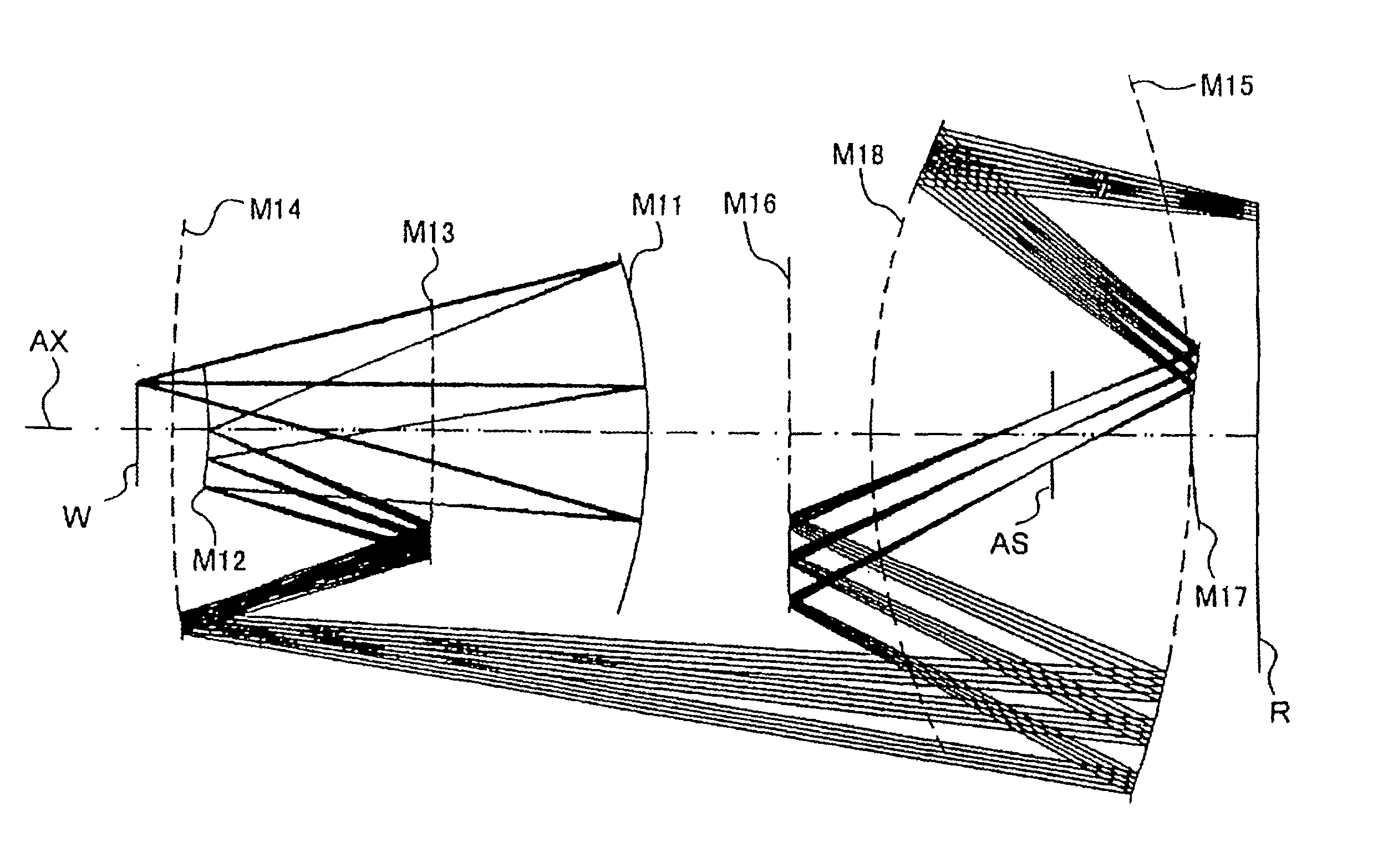
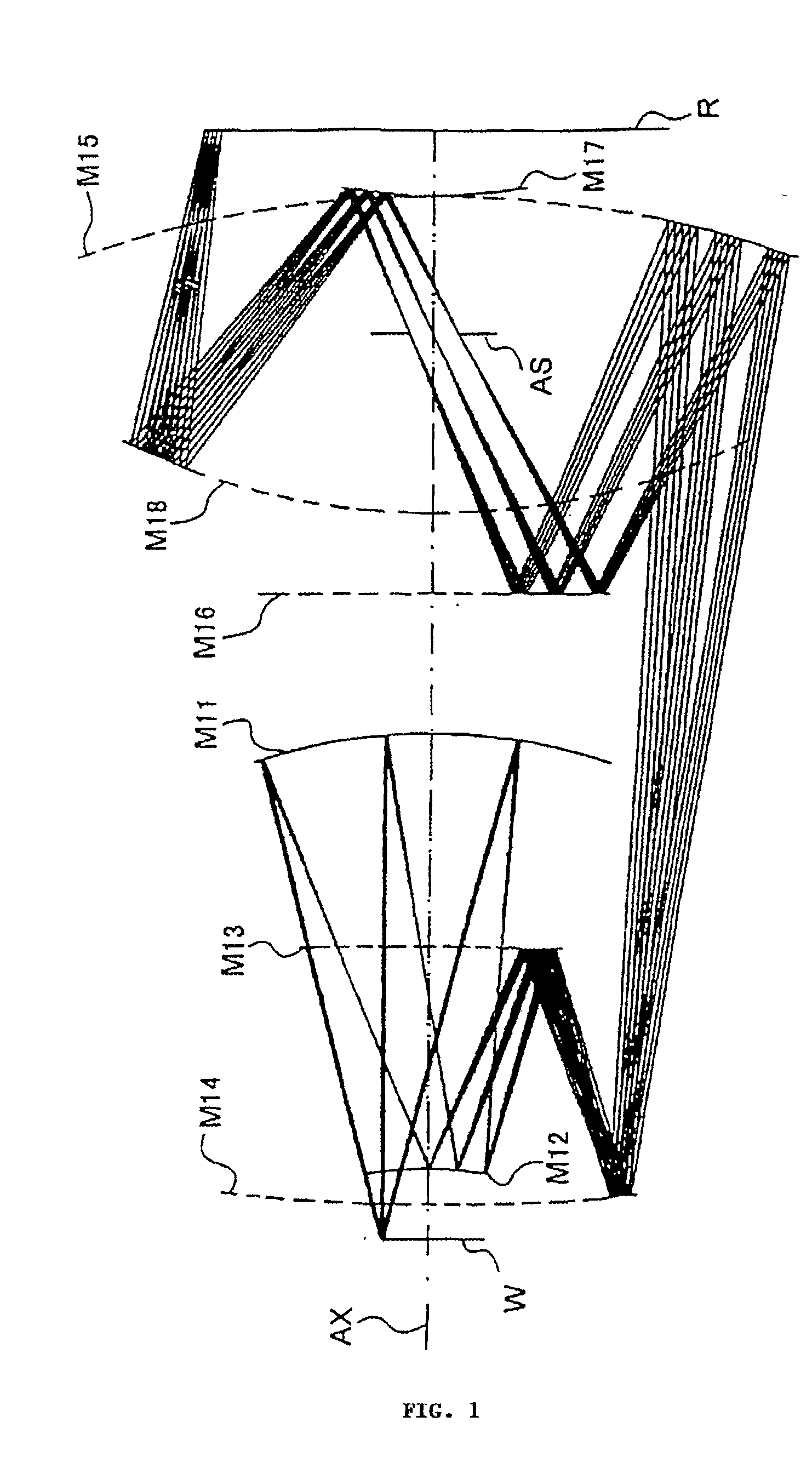
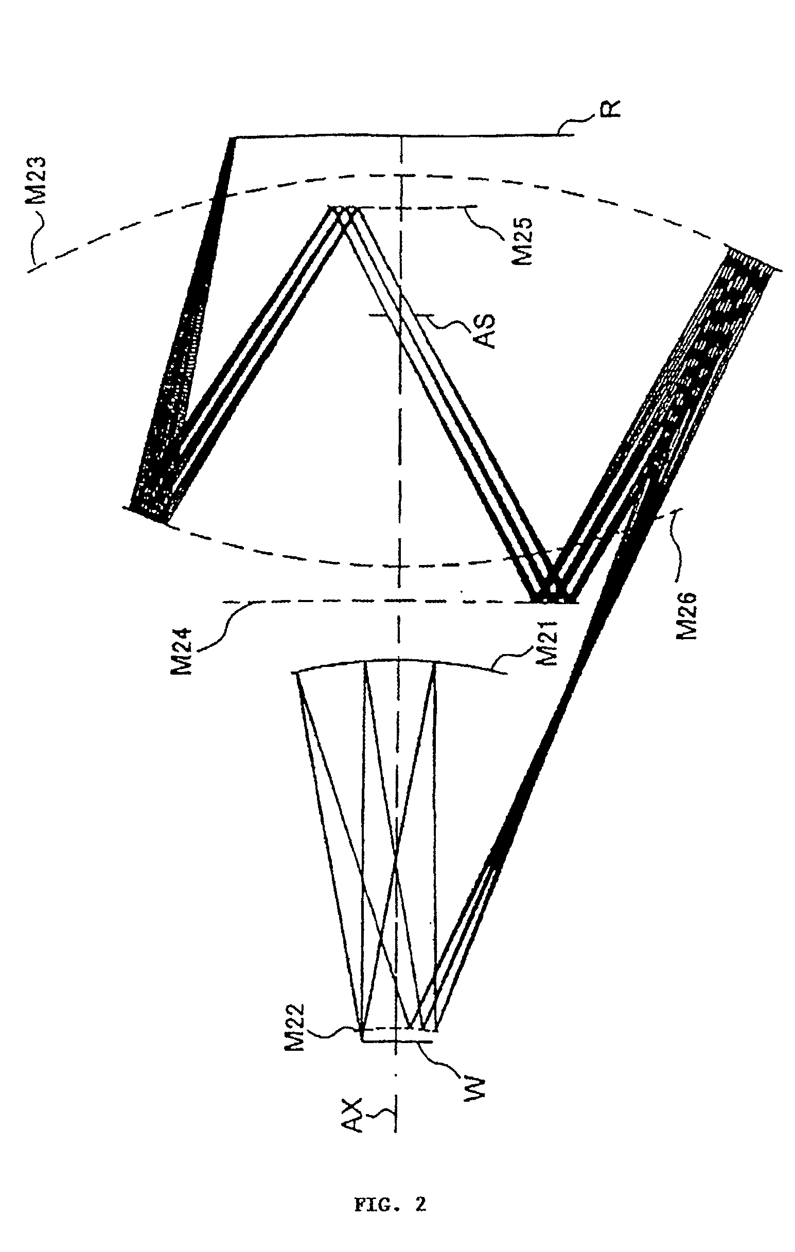
  • Imaging optical system and exposure apparatus
  • Imaging optical system and exposure apparatus
  • Imaging optical system and exposure apparatus

Examples


Embodiment Construction

[0001] 1. Cross-Reference To Related Application and Claim of Foreign Priority Date

[0002] This application claims right of benefit of prior filing date of Japanese Patent Application No. H13-305521 (2001), filed 1 Oct. 2001, entitled Imaging Optical System and Exposure Apparatus," the content of which is incorporated herein by reference in its entirety.

[0003] 2. Field of the Invention

[0004] The present invention pertains to an imaging optical system and exposure apparatus which may be favorably used during manufacture for example of semiconductor elements, liquid crystal display elements, image pickup elements, CCD elements, thin-film magnetic heads, and / or other such microdevices through use of photolithographic techniques.

[0005] 3. Background of the Invention

[0006] Minimum linewidths in circuit patterns grow smaller with each successive generation of technology in the semiconductor and like fields of art. With each such generation of technology, greater resolving power has therefo...


PUM

PropertyMeasurementUnit
wavelengthaaaaaaaaaa
wavelengthsaaaaaaaaaa
wavelengthaaaaaaaaaa

Abstract

An imaging optical system may be capable of forming substantially in one or more second planes one or more complete and / or partial images of one or more objects arranged substantially in one or more first planes and may comprise one or more entrance pupils, at least one of which is located substantially on an opposite side of at least one of the first plane or planes from the imaging optical system exclusive of the at least one entrance pupil so located. Such imaging optical system may be constructed so as to be substantially telecentric on at least a same side thereof as at least one of the second plane or planes. Such imaging optical system may be such that all of the reflective surface or surfaces of the imaging optical system are located in one or more spaces substantially between at least one of the first plane or planes and at least one of the second plane or planes, inclusive, and / or such imaging optical system may further comprise one or more locations disposed in one or more optical paths from at least one of the first plane or planes to at least one of the second plane or planes, inclusive, and substantially optically conjugate to at least one of the first plane or planes.

Description

DESCRIPTION OF THE INVENTION[0001] 1. Cross-Reference To Related Application and Claim of Foreign Priority Date[0002] This application claims right of benefit of prior filing date of Japanese Patent Application No. H13-305521 (2001), filed 1 Oct. 2001, entitled Imaging Optical System and Exposure Apparatus," the content of which is incorporated herein by reference in its entirety.[0003] 2. Field of the Invention[0004] The present invention pertains to an imaging optical system and exposure apparatus which may be favorably used during manufacture for example of semiconductor elements, liquid crystal display elements, image pickup elements, CCD elements, thin-film magnetic heads, and / or other such microdevices through use of photolithographic techniques.[0005] 3. Background of the Invention[0006] Minimum linewidths in circuit patterns grow smaller with each successive generation of technology in the semiconductor and like fields of art. With each such generation of technology, greater...

Claims


Application Information

Patent Timeline
Patent Type & Authority Applications(United States)
IPC IPC(8): G02B27/18G02B17/00G03B27/42G03F7/20H01L21/027
CPCG03F7/70233G03B27/42
Inventor KOMATSUDA, HIDEKI
Owner NIKON CORP
Learn More