Pin-assignment method for integrated circuit packages to increase the electro-static discharge protective capability thereof

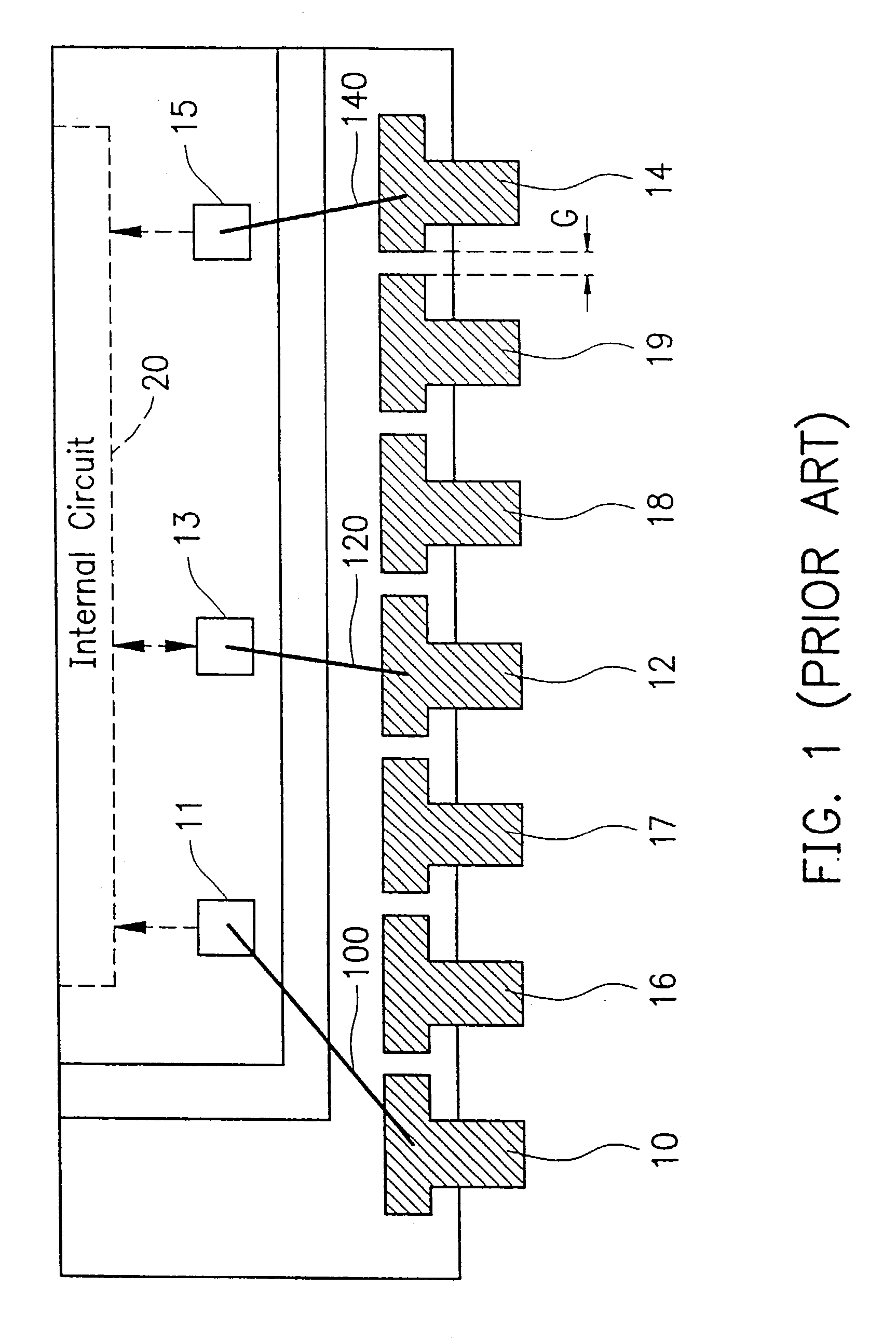
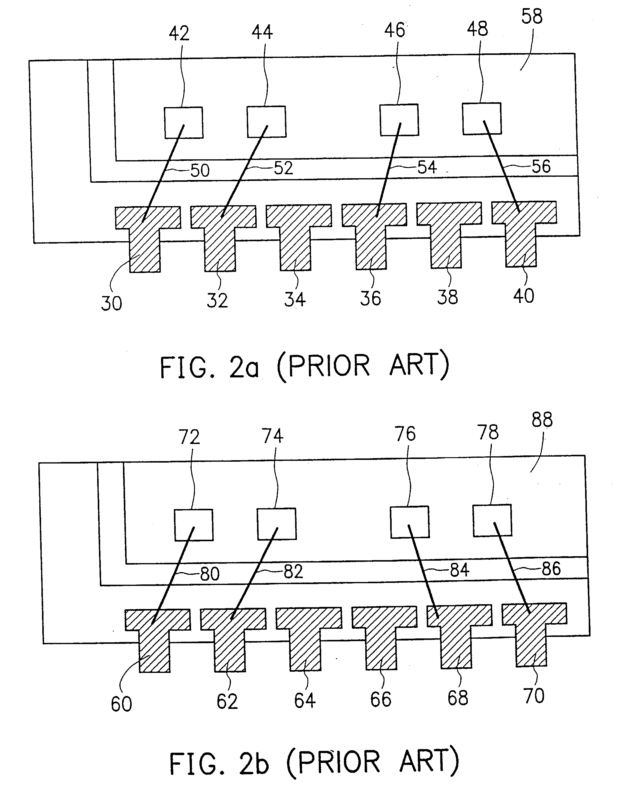
a technology of integrated circuits and pin assignments, which is applied in the direction of solid-state devices, electric devices, electrical equipment, etc., can solve the problems of esd damage, ic chip damage, esd damage is particularly common and severe,

Inactive Publication Date: 2003-06-05
WINBOND ELECTRONICS CORP
View PDF0 Cites 7 Cited by
  • Summary
  • Abstract
  • Description
  • Claims
  • Application Information

AI Technical Summary

Problems solved by technology

Electrostatic discharge (ESD) is a movement of static electricity from a nonconductive surface, which usually causes damage to the semiconductors and various other circuit components in IC chips.
If such a person touches an IC chip by hand, the electrostaticity on his / her body would instantaneously be discharged to the IC chip, thus causing damage to the IC chip.
The ESD damage is particularly common and severe on CMOS (complementary metal-oxide semiconductor) IC devices.
The reduction of the pin gap, however, causes a new problem in ESD protection for the IC package.
This paper reveals the fact that, when a human body model (HBM) ESD pulse is repeatedly applied to a certain no-connect pin on the IC package, any of its two neighboring pins, if wired to the internal circuit, would become particularly vulnerable to ESD damage.
This is because that the electrostatic charge will accumulate in the resin around the no-connect pin, thus resulting in a large potential difference between the no-connect pin and its neighboring pins, thus significantly reducing the ESD resistant capability of the neighboring pins.
Early types of IC packages have only a small number of pins thereon, so the above-mentioned proximity problem that would cause ESD damage is unobvious.
With such a large number of pins on a small-size IC package, the above-mentioned proximity problem becomes a serious consideration.
One drawback to this solution, however, is that the ESD protective circuitry needed to provide such an ESD protective capability will take up more area on the IC chip, thus increasing the chip size.
The input pins, I / O pins and output pins are inferior to the power pins in ESD protective capability.
Therefore, when these pin-assignment methods are utilized on IC packages with a high density of pins, the arrangement of the no-connect pins next to ESD-sensitive pins could cause the problem of ESD damage.

Method used


Image

  • Pin-assignment method for integrated circuit packages to increase the electro-static discharge protective capability thereof
  • Pin-assignment method for integrated circuit packages to increase the electro-static discharge protective capability thereof
  • Pin-assignment method for integrated circuit packages to increase the electro-static discharge protective capability thereof

Examples


Embodiment Construction

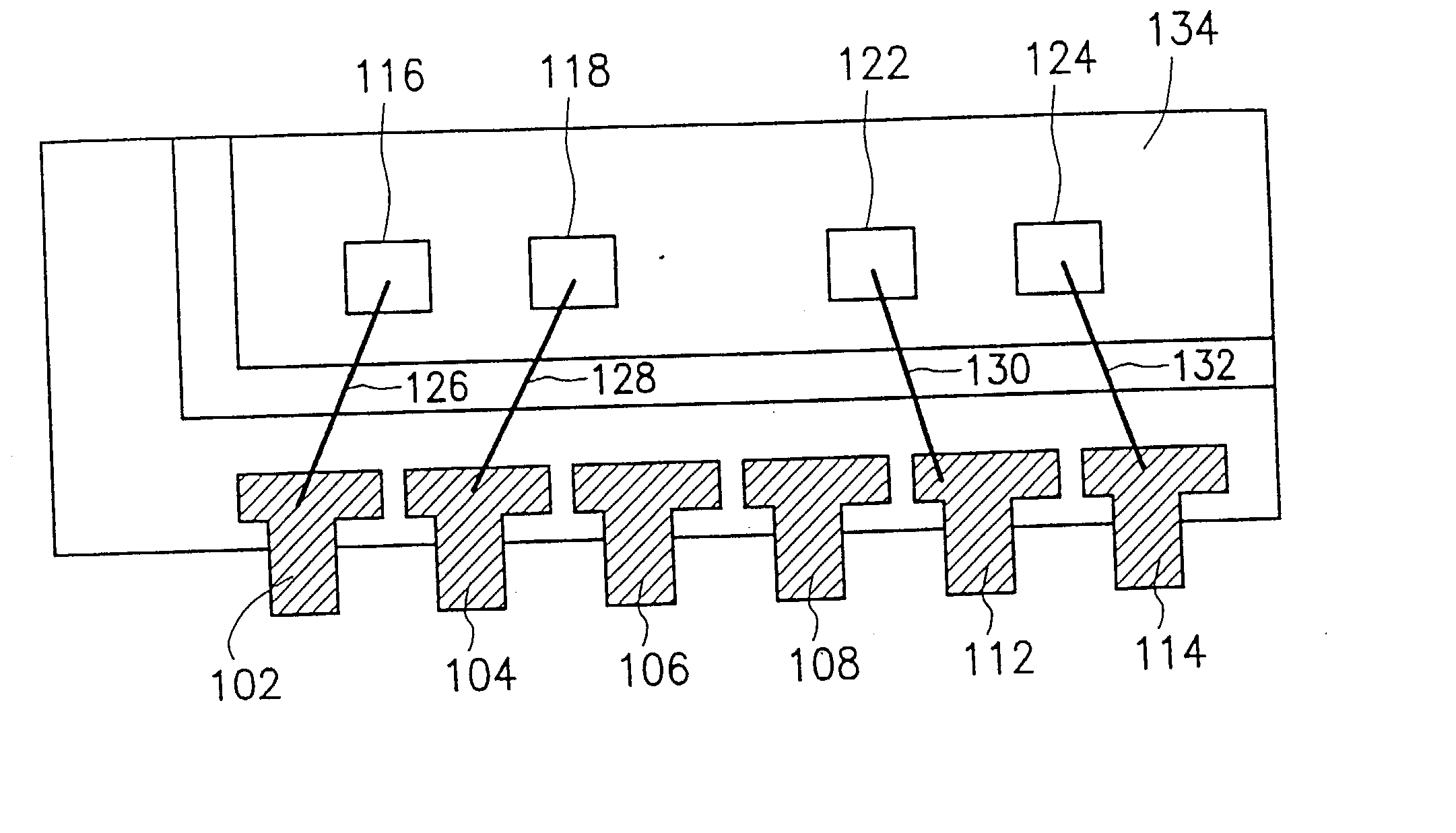
[0024] In accordance with the invention, the pins of an IC package are organized in such a manner that the no-connect pins are set apart into a plurality of groups or at least one group, with each group containing one single no-connect pin or a number of consecutive no-connect pins, and then each of the two pins that bound both sides of each no-connect pin group is assigned to be a power pin, such as a power pin V.sub.DD, a power pin V.sub.SS, or a ground pin GND, for electrically connect to a power bus V.sub.DD, a power bus V.sub.SS, or a ground bus GND of the IC chip. This arrangement is based on the fact that the pins that are connected to a power bus can better withstand the condition of its neighboring no-connect pin being subjected to an ESD stress of 5 kV. Therefore, in this case, the ESD protective circuitry for the power pins needs not be expanded while nonetheless retaining good ESD protective capability. 7File:

[0025] FIG. 3 is a schematic diagram depicting the pin-assignm...


PUM


Abstract

A pin-assignment method is provided for use on an IC package to arrange pin connections. The pin-assignment method can allow an improvement in the electro-static discharge (ESD) protection capability for the IC chip packed in the IC package. Specifically, the pin-assignment method organizes the no-connect pins of the IC package into groups and then assigns each of the two pins that bound each no-connect pin group to be connected to a power bus of the IC chip. This allows for an increased ESD protective capability for the no-connect pins. Moreover, the pin-assignment method can simplify the wiring complexity of the IC package.

Description

[0001] This application claims the priority benefit of Taiwan application serial no. 86115577, filed Oct. 22, 1997, the fill disclosure of which is incorporated herein by reference.[0002] 1. Field of the Invention[0003] This invention relates in general to a pin-assignment method for integrated circuit (IC) packages, which can allow an increase in the electro-static discharge (ESD) protective capability for the IC chip packed in the IC package. Specifically, the pin-assignment method organizes the no-connect pins of the IC package into groups and then assigns each of the two pins that bound each no-connect pin group to be connected to a power line, whereby the IC chip can be increased in its ESD protective capability and simplified in its wiring complexity.[0004] 2. Description of Related Art[0005] Electrostatic discharge (ESD) is a movement of static electricity from a nonconductive surface, which usually causes damage to the semiconductors and various other circuit components in I...

Claims


Application Information

Patent Timeline
Patent Type & Authority Applications(United States)
IPC IPC(8): H01L23/60
CPCH01L23/60H01L2224/48247H01L2224/49112H01L2224/49171H01L2924/14H01L24/49H01L24/48H01L2924/00H01L2224/05553H01L2224/05554H01L2224/05599H01L2224/85399H01L2924/00014H01L2224/45099H01L2224/45015H01L2924/207
Inventor LIN, SHI-TRON
Owner WINBOND ELECTRONICS CORP
Why Eureka
Try Eureka