Method of manufacturing a flash memory cell

a technology of flash memory and manufacturing method, which is applied in the direction of semiconductor devices, electrical apparatus, transistors, etc., can solve the problems of memory cell erase failure, poor uniformity of wafer, and difficulty in implementing a uniform floating ga

Inactive Publication Date: 2003-06-26
SK HYNIX INC
View PDF9 Cites 21 Cited by
  • Summary
  • Abstract
  • Description
  • Claims
  • Application Information

AI Technical Summary

Benefits of technology

[0006] A method of manufacturing a flash memory cell is disclosed wherein a device of a smaller size can be implemented while the coupling ratio of a floating gate is obtained by maximum, in a way that a trench insulating film is etched by a desired space by controlling a wall sacrificial oxidization process, a wall oxidization process and a cleaning process for the trench insulating film that are performed before and after a process of forming the trench insulating film for burying a trench is performed.

Problems solved by technology

During the process of isolating a floating gate using mask patterning, wafer uniformity is very poor depending on variation in a mask critical dimension (CD).
It is thus difficult to implement a uniform floating gate.
Further, there are problems such as program and erase fail of the memory cell, or the like, depending on variation in the coupling ratio.
In addition, in a higher-integrated design, when a space of below 0.13 .mu.m is implemented, the masking process is difficult.
Thus, a process of manufacturing the flash memory cell serving as an important factor in implementing a uniform floating gate becomes further difficult.
Also, if the floating gate is not uniformly formed, difference in the coupling ratio becomes severe.
This adversely affects a device characteristic.
Also, the yield of the product is lowered and the cost is increased, due to increase in the mask process.

Method used


Image

  • Method of manufacturing a flash memory cell
  • Method of manufacturing a flash memory cell
  • Method of manufacturing a flash memory cell

Examples


Embodiment Construction

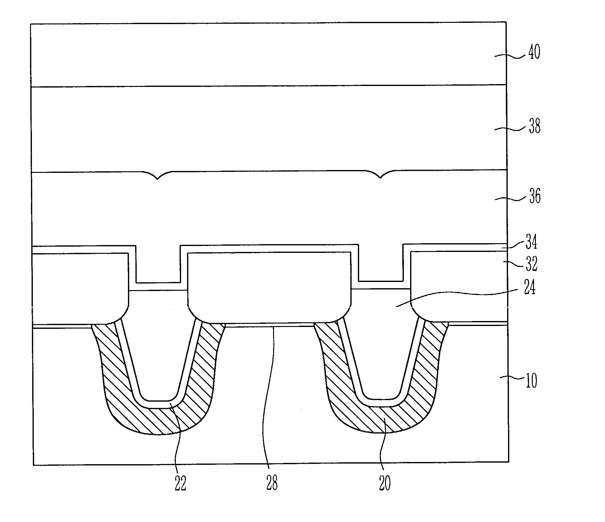
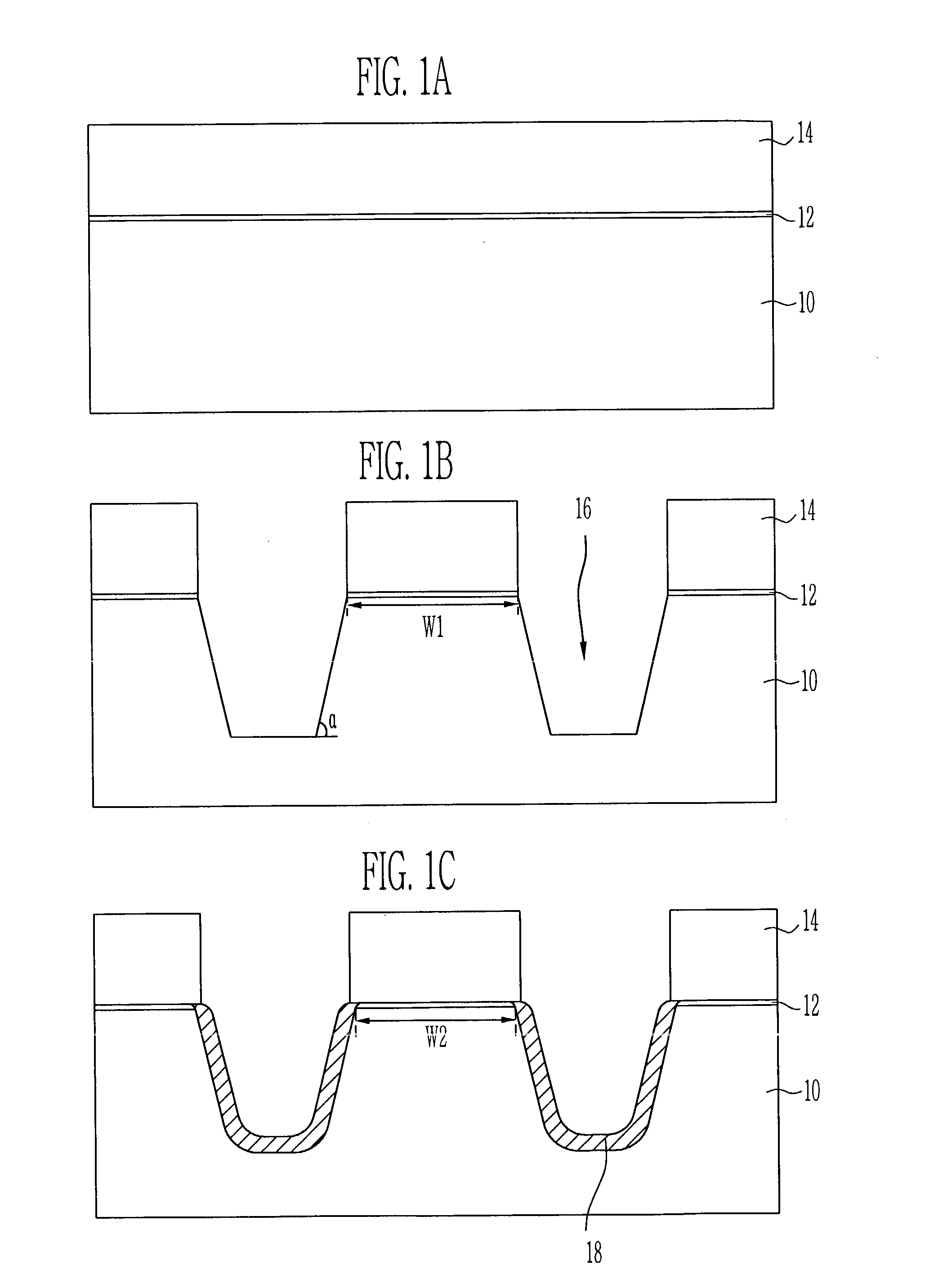
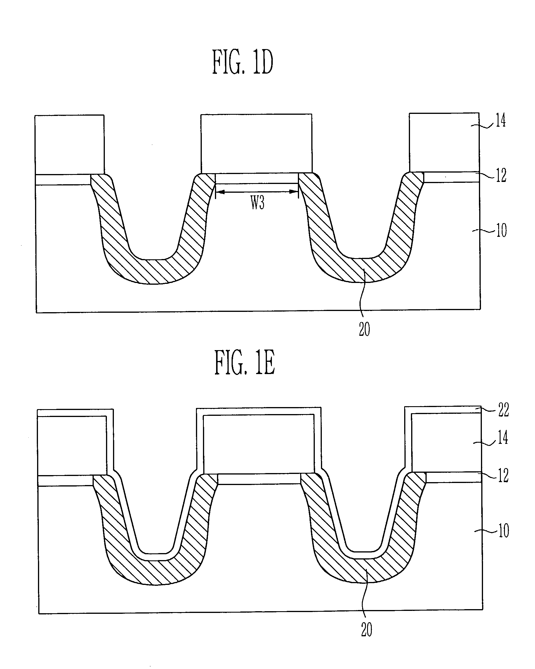
[0010] FIG. 1A through FIG. 1L are cross-sectional views of flash memory cells for describing a method of manufacturing the flash memory cell according to a preferred embodiment.

[0011] Referring now to FIG. 1A, a pad oxide film 12 and a pad nitride film 14 are sequentially formed on a semiconductor substrate 10.

[0012] At this time, the pad oxide film 12 is formed in thickness of 70 through 200 .ANG. by dry or wet oxidization process at a temperature ranging from about 700 to about 950.degree. C. in order to prohibit crystal defects on the surface of the semiconductor substrate 10 or mitigate stress of the pad nitride film 14 to be formed in a surface processing or subsequent process. Further, the pad nitride film 14 is formed to be relatively thick, i.e., from about 2000 to about 3500 .ANG., by means of a LP-CVD method.

[0013] Referring now to FIG. 1B, a STI process using an isolation (ISO) mask is performed to etch a given portion of the semiconductor substrate 10 including the pad ...


PUM


Abstract

A method of manufacturing a flash memory cell. The method includes controlling a wall sacrificial oxidization process, a wall oxidization process and a cleaning process of a trench insulating film that are performed before / after a process of forming the trench insulating film for burying a trench to etch the trench insulating film to a desired space. Therefore, it is possible to secure the coupling ratio of a floating gate by maximum and implement a device of a smaller size.

Description

[0001] 1. Technical Field[0002] Methods of manufacturing flash memory cells, and more particularly to, methods of forming a self-aligned floating gate capable of increasing the coupling ratio of flash memory cells are disclosed.[0003] 2. Description of the Related Art[0004] Generally, a flash memory cell is implemented using a shallow trench isolation (STI) process as a device isolation process. During the process of isolating a floating gate using mask patterning, wafer uniformity is very poor depending on variation in a mask critical dimension (CD). It is thus difficult to implement a uniform floating gate. Further, there are problems such as program and erase fail of the memory cell, or the like, depending on variation in the coupling ratio.[0005] In addition, in a higher-integrated design, when a space of below 0.13 .mu.m is implemented, the masking process is difficult. Thus, a process of manufacturing the flash memory cell serving as an important factor in implementing a unifo...

Claims


Application Information

Patent Timeline
Patent Type & Authority Applications(United States)
IPC IPC(8): H01L21/762H01L21/8247H01L27/115H01L29/788H01L29/792
CPCH01L27/11521H01L21/76235H10B41/30H10B69/00
Inventor KIM, JUM SOOJUNG, SUNG MUNAHN, JUNG RYULSHIN, YOUNG KILEE, YOUNG BOK
Owner SK HYNIX INC
Why Eureka
Try Eureka