Multi-chip stack package and fabricating method thereof

a technology of multi-chip stacks and fabrication methods, applied in the direction of semiconductor devices, semiconductor/solid-state device details, electrical devices, etc., can solve the problem of adhesive material 150 bleedout, and achieve the effect of improving the bonding quality of multi-chip stacks

Inactive Publication Date: 2003-07-10
ADVANCED SEMICON ENG INC
View PDF7 Cites 21 Cited by
  • Summary
  • Abstract
  • Description
  • Claims
  • Application Information

AI Technical Summary

Benefits of technology

0008] Accordingly, one object of the present invention is to provide a multi-chip stack package and a fabricating method thereof that can improve bonding quality of the multi-chip stack.

Problems solved by technology

However, if too much attaching pressure is applied to the second chip 140, some adhesive material 150 will bleed out.

Method used


Image

  • Multi-chip stack package and fabricating method thereof
  • Multi-chip stack package and fabricating method thereof
  • Multi-chip stack package and fabricating method thereof

Examples


Embodiment Construction

[0021] Reference will now be made in detail to the present preferred embodiments of the invention, examples of which are illustrated in the accompanying drawings. Wherever possible, the same reference numbers are used in the drawings and the description to refer to the same or similar parts.

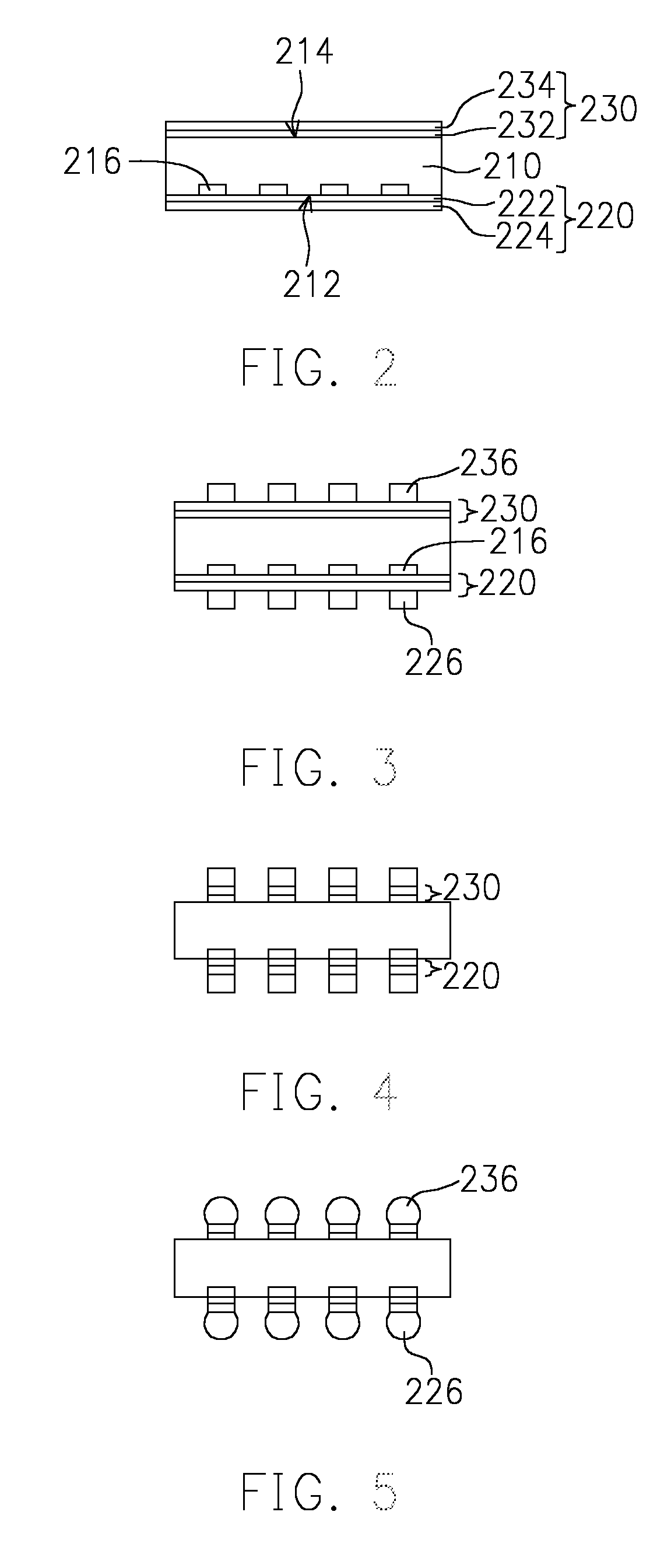
[0022] Figs. 2 to 11 are schematic cross-sectional views showing the progression of steps for fabricating a multi-chip stack package according to a first preferred embodiment of this invention. As shown in Fig. 2, a first chip 210 having a first active surface 212 and a first chip back surface 214 is provided. The first chip 210 further includes a plurality of first bonding pads 216 positioned on the first active surface 212 of the first chip 210. Thereafter, a process is carried out to form an under-bump-metallurgy layer. To form the under-bump-metallurgy layer, a sputtering process is conducted to form a first barrier layer 222 and a second barrier layer 232 over the first active surface 212 an...


PUM


Abstract

Abstract of Disclosure A multi-chip stack package having a substrate, a first chip, a second chip, a plurality of bumps, a plurality of junction interface bumps, a plurality of conductive wires, a first filler material, a second filler material and an encapsulating material is provided. The substrate has a substrate surface with a plurality of first contacts and a plurality of second contacts. The first chip has a first active surface with a plurality of bonding pads thereon and a first chip back surface. The first chip is positioned over the substrate surface. The second chip has a second active surface with a plurality of bonding pads thereon and a second chip back surface. The second chip is positioned over the first chip back surface. The bumps are positioned between the first bonding pads and the first contacts. The junction interface bumps are positioned between the first chip back surface and the second chip back surface. The conductive wires electrically connect the second bonding pads and the second contacts. The first filler material encloses the bumps and the second filler material encloses the junction interface bumps. The encapsulating material encloses the first chip, the second chip and the conductive wires.

Description

Cross Reference to Related Applications[0001] This application claims the priority benefit of Taiwan application serial no. 91100096, filed January 7, 2002.Background of Invention[0002] Field of Invention[0003] The present invention relates to a multi-chip stack package. More particularly, the present invention relates to a multi-chip stack package and fabricating method thereof that can improve the quality of a multi-chip stack package.[0004] Description of Related Art[0005] As electronic technologies continue to advance, more personalized, multi-functional high-tech electronic products are being introduced into the market. The newer electronic products are characteristically smaller, lighter and slimmer so that the product will occupy less space and be more portable. In semiconductor manufacturing, many types of packages now incorporate a multi-chip concept so that volume occupation of an integrated circuit is reduced and electrical performance is improved. In a multi-chip stack p...

Claims


Application Information

Patent Timeline
Patent Type & Authority Applications(United States)
IPC IPC(8): H01L25/065
CPCH01L24/17H01L2224/81193H01L24/73H01L25/0657H01L2224/16145H01L2224/16225H01L2224/48091H01L2224/48227H01L2224/73265H01L2225/0651H01L2225/06513H01L2225/06517H01L2225/06582H01L2924/01029H01L2924/0105H01L2924/01082H01L24/32H01L2224/73257H01L2224/14181H01L2224/73204H01L2224/32225H01L2224/32145H01L2924/014H01L2924/01074H01L2924/01033H01L2924/01024H01L2924/00014H01L2924/00H01L2924/00012H01L2924/14H01L2224/05571H01L2224/05573H01L2224/05001H01L2224/0508H01L2224/05568H01L2224/05023H01L2224/17181H01L24/05H01L24/13H01L24/16
Inventor FANG , JEN-KUANG
Owner ADVANCED SEMICON ENG INC
Why Eureka
Try Eureka