Optical fiber and optical fiber wiring board using the optical fiber

Inactive Publication Date: 2003-08-07
MITSUBISHI CABLE IND LTD +1
1 Cites 0 Cited by

AI-Extracted Technical Summary

Problems solved by technology

However, a problem arises in that such a routing manner makes it difficult to implement the miniaturization of the optical-fiber wiring board.
However, when the upper optical fiber is routed to have a radius of curvature greater than the minimum radius of curvature, mutual interference occurs between the upper optical fiber and other optical fibers routed adjacent to the lower optical fiber routed on the substrate.
In order to achieve the reduction, however, the area of the substrate needs to be enlarged, which consequently leads to enlargement o...

Benefits of technology

0031] As described above, since the optical fiber routed on the substrate of the optical-fiber wiring board has the relative refraction index difference that is greater than the relative refraction index difference of the communication-dedicated single mode optical fiber, the bending loss is reduced. Therefore, the bending loss is not increased even when the optical fiber is routed at a small radius of curvature on the substrate. The bending loss is not increased also in the crossover section where the two optical fibers cross over one another. Consequently, miniaturization can be implemented for the optical-fiber wiring board. Further, since t...

Abstract

Optical fibers (220) are routed over a substrate (210), and an optical fiber wiring board (200) is thereby constructed. A relative refraction index difference DELTA of the optical fiber (220) is increased to be greater than a relative refraction index difference DELTA0 of a communication-dedicated single mode optical fiber, and a core diameter thereof is increased to be larger than a core diameter of the communication-dedicated optical fiber. Thereby, a mode field diameter thereof is set to be substantially the same as a mode field diameter of the communication-dedicated optical fiber.

Application Domain

Optical fibre with graded refractive index core/claddingCoupling light guides +1

Technology Topic

Mode field diameterMulti-mode optical fiber +4

Image

  • Optical fiber and optical fiber wiring board using the optical fiber
  • Optical fiber and optical fiber wiring board using the optical fiber
  • Optical fiber and optical fiber wiring board using the optical fiber

Examples

  • Experimental program(1)

Example

[0046] FIG. 1 shows an example of an optical matrix conversion wiring board 100 according to an embodiment of the present invention. The optical matrix conversion wiring board is an optical-fiber wiring board that converts inputs of m ports and n channels (hereinafter, referred to as "(m, n) inputs". It is noted that the letters "m" and "n" each represents a natural number) into outputs of n ports and m channels (hereinafter, referred to as "(n, m) outputs"). The optical matrix conversion wiring board 100 (hereinafter, referred to as an m.times.n optical matrix conversion wiring board) has advantages in that a number of optical fibers are arranged in units of a channel, thereby preventing erroneous wiring, and in that the optical fibers are routed on a plane, whereby a reduced storage area suffices for installation.
[0047] The optical matrix conversion wiring board 100 shown in FIG. 1 includes 16 input terminals and 16 output terminals, and it is constructed to be a 16.times.16 optical matrix conversion wiring board for converting (I to XVI, 1 to 16) inputs to (1 to 16, I to XVI) outputs. In FIG. 1, input terminals and output terminals are partly omitted for illustration. The optical matrix conversion wiring board 100 is constructed of first to forth sub-wiring boards 200 to 500 laminated one above the other.
[0048] As shown in FIG. 2, each of the sub-wiring boards 200 to 500 (first sub-wiring board 200 in FIG. 2) is constructed of a substrate 210 and optical fibers 220 routed on the substrate 210. In addition, as shown in FIG. 1, each of the sub-wiring boards 200 to 500 includes input-side optical connectors 231 to which the input terminals are connected and output-side optical connectors 241 to which the output terminals are connected. The input-side optical connectors 231 and the output-side optical connectors 241 are individually formed of 8-conductor MT connectors. On each of the sub-wiring boards 200 to 500, since 64 optical fibers 220 are routed, eight input-side optical connectors 231 and eight output-side optical connectors 241 are provided on each of the sub-wiring boards 200 to 500. The optical connectors 231 and 241 are not limited to the 8-conductor connectors, but may be other multi-conductor connectors.
[0049] In the optical matrix conversion wiring board 100, (I to VIII, 1 to 8) inputs and (1 to 8, I to VIII) outputs are connected on the first sub-wiring board 200, and (I to VIII, 9 to 16) inputs and (9 to 16, I to VIII) outputs are connected on the second sub-wiring board 300. In addition, (IX to XVI, 1 to 8) inputs and (1 to 8, IX to XVI) outputs are connected on the third sub-wiring board 400, and (IX to XVI, 9 to 16) inputs and (9 to 16, IX to XVI) outputs are connected on the fourth sub-wiring board 500. According to the above-described construction, on the optical matrix conversion wiring board 100, the (I to XVI, 1 to 16) inputs are fed to the individual input-side optical connectors 231 of the fist to fourth sub-wiring boards 200 to 500 via the input terminals. In addition, the (1 to 16, I to XVI) outputs are obtained from the individual output-side optical connectors 241 of the first to fourth sub-wiring boards 200 to 500 via the output terminals.
[0050] Hereinafter, the structures of the individual sub-wiring boards 200 to 500 will be described in detail with reference to FIGS. 2 and 3. The first to fourth sub-wiring boards 200 to 500 have same structures with one another, except that the fiber-routing patterns of the optical fibers 220 are different. As such, hereinafter, description will be given of the first sub-wiring board 200 as an example.
[0051] The first sub-wiring board 200 includes the substrate 210 on which an adhesive layer 211 is formed, and the optical fiber 220 is adhered to the adhesive layer 211 and is thereby fixed to the substrate 210.
[0052] A material having a high resistance against vibration is preferably used for the substrate 210 to prevent the routed optical fiber 220 from easily being deflected. As a material for forming the substrate 210, for example, a polyimide resin, a polyethylene terephthalate resin or a polyethylene naphthalate resin may be used.
[0053] The adhesive layer 211 is a layer having tackiness or adhesion property, and it may be any layer capable of securely fixing the optical fiber 220. The adhesive layer 211 may therefore be formed using a known pressure sensitive adhesive or an adhesive (such as a silicone adhesive).
[0054] In the sub-wiring board 200 thus formed, the optical fibers 220 routed on the substrate 210 may be covered by a laminate layer (not shown). This enables the optical fibers 220 to be protected from outside forces and humidity. In addition, the fiber-routing stability is enhanced, thereby improving the reliability. As the laminate layer, polytetrafluoroethylene (PTFE) or the like may be used.
[0055] In addition, on the first sub-wiring board 200, eight optical fibers 220 are connected to each of the input-side optical connectors 231, and each optical fiber bundle 232 is formed such that the eight optical fibers 220 are routed in close contact with one another. Accordingly, eight input-side optical fiber bundles 232 are provided.
[0056] Each of the input-side optical fiber bundles 232 is routed in a predetermined fiber-routing pattern on the substrate 210 in a portion from an input-side edge portion of the substrate 210 to the vicinity of a central portion thereof. Specifically, in a portion from an input-side edge portion of the substrate 210 to the vicinity of a central portion thereof, each of the optical fiber bundles 232 is routed on the substrate 210 in such a manner as to form linear portions extending in the X direction and the Y direction and curved portions 251 to 254 (radii of curvature R1 to R4) curved to be a 1/4 circular arc shape.
[0057] In the vicinity of the central portion of the substrate 210, the optical fibers 220 constituting the each of the optical fiber bundles 232 are separated one by one. At this time, each of the optical fibers 220 is routed in such a manner as to form a curved portion 255 having a radius of curvature R5.
[0058] In the vicinity of the central portion of the substrate 210, the individual optical fibers 220 separated from the one optical fiber bundle 232 are routed in close contact with individual optical fibers 220 separated from seven other optical fiber bundles 232. Thereby, eight output-side optical fiber bundles 242, each of which includes eight optical fibers 220 as one bundle, are formed. In this manner, the input-side optical fiber bundles 232 individually corresponding to channels (ch 1 to 8) including ports I to VIII are restructured into the output-side optical fiber bundles 242 individually corresponding to channels (ch I to VIII) including ports 1 to 8. For example, each of the optical fibers 220 of the input-side ch 1 is included in the ports 1 of the output-side ch I to VIII.
[0059] Also similar to the input-side optical fiber bundle 232, each of the output-side optical fiber bundle 242 is routed in a predetermined fiber-routing pattern on the substrate 210 in the portion from the vicinity of a central portion of the substrate 210 to an output-side edge portion thereof. More specifically, in a portion from the vicinity of a central portion of the substrate 210 to an output-side edge portion thereof, each of the optical fiber bundles 242 is routed on the substrate 210 in such a manner as to form linear portions extending in the X direction and the Y direction and curved portions 256 to 258 (radii of curvature R6 to R8) curved to be a 1/4 circular arc shape. In addition, the output-side optical connectors 241 are individually connected to the eight output-side optical fiber bundles 242.
[0060] The first sub-wiring board 200 may preferably be manufactured using, for example, an X-Y plotter (not shown). Specifically, a fiber-routing head of the X-Y plotter is moved along the predetermined fiber-routing pattern on the substrate 210, and concurrently, the optical fiber 220 is provided onto the substrate 210 (adhesive layer 211) via the fiber-routing head. At this time, the provided optical fiber 220 is pressed at a predetermined force onto the adhesive layer 211, and the optical fiber 220 is thereby adhered to the adhesive layer 211. Thus, the optical fiber 220 is routed in the predetermined fiber-routing pattern on the substrate 210. These steps are repeatedly performed for all the 64 optical fibers 220, thereby enabling the first sub-wiring board 200 as shown in FIG. 2 to be manufactured.
[0061] The first sub-wiring board 200 (optical matrix conversion wiring board 100) includes, for example, many crossover sections 259 in each of which two optical fibers 220 routed in such a manner as to cross over one another on the substrate 210, and a number of curved portions 251 to 258 in each of which the optical fiber 220 is routed in such a manner as to be curved to be the 1/4 circular arc shape.
[0062] As shown in FIG. 3, a lower optical fiber 220a is adhered onto the adhesive layer 211 in the crossover section 259. On the other hand, an upper optical fiber 220b is disposed in contact with the lower optical fiber 220a and to cross over the lower optical fiber 220a. In addition, the upper optical fiber 220b is disposed in such a manner as to have a predetermined radius of curvature Ra. The radius of curvature Ra is set to be greater than the minimum radius of curvature allowable with respect to the bending loss of the optical fiber 220.
[0063] Similarly, in the individual curved portions 251 to 258, each of the radii of curvature R1 to R8 of the individual optical fibers 220 is set to be greater than the minimum radius of curvature. Each of the curved portions 251 to 258 need not necessarily be in the circular arc shape, and the optical fiber 220 may instead be formed in such a manner as to have a radius of curvature greater than the minimum radius of curvature.
[0064] Hereinafter, the optical fibers 220 used with the optical matrix conversion wiring board 100 will be described. In comparison to an ordinarily communication-dedicated single mode optical fiber, the optical fiber 220 is shorter in the overall length. As such, dissimilar to the communication-dedicated single mode optical fiber, the optical fiber 220 is designed without considering dispersion as a design parameter.
[0065] In specific, for the optical fiber 220, a relative refraction index difference .DELTA. [%] of a core and a cladding and a core diameter thereof are set in such a manner that a mode field diameter (MFD) and a cut-off wavelength .lambda.c individually take predetermined values.
[0066] That is, as shown in FIG. 4, the core diameter, the MFD, the cut-off wavelength .lambda.c, and the relative refraction index difference .DELTA., which are design parameters of the optical fiber, are related to one another. When the cut-off wavelength .lambda.c and the MFD are set, the relative refraction index difference .DELTA. and the core diameter are individually determined according thereto. For example, as shown in FIG. 5, in the case of a communication-dedicated single mode optical fiber according to the ITU standards, when the wavelength of propagated light is 1.3 .mu.m, the cut-off wavelength .lambda.c is determined to be 1.1 to 1.28 .mu.m, and the MFD is determined to be 9.5.+-.0.5 .mu.m (G652). Thereby, the relative refraction index difference .DELTA. of the optical fiber is determined to be 0.36%, and the core diameter thereof is determined to be 8 .mu.m. When the wavelength of propagated light is 1.55 .mu.m, an ordinary communication-dedicated single mode optical fiber is designed to have an MFD of 10.5.+-.0.5 .mu.m (it is noted that this value is a standard value, not a specification value). Accordingly, the relative refraction index difference .DELTA. is determined to be 0.36%, and the core diameter is determined to be 8 .mu.m.
[0067] In comparison to the above, the optical fiber 220 is designed to have a relative refraction index difference .DELTA. greater than a relative refraction index difference (hereinafter, referred to as an ordinary relative refraction index difference .DELTA..sub.0 [%]) of the normal communication-dedicated single mode optical fiber. Thereby, the optical fiber 220 is imparted with an enhanced confinement of light into the core. Consequently, even when the optical fiber 220 is bent, it is suppressed that light in the core transmit to the cladding. That is, the optical fiber 220 reduces the bending loss.
[0068] Generally, when the relative refraction index difference .DELTA. is greater than the ordinary relative refraction index difference .DELTA..sub.0, the MFD of the optical fiber is less than the MFD of the ordinary communication-dedicated single mode optical fiber (hereinafter, referred to as an ordinary MFD). In this state, when the optical fiber is connected to the ordinary communication-dedicated single mode optical fiber, the connection loss is increased. For this reason, the core diameter of the optical fiber 220 is increased to be larger than the core diameter of the ordinary communication-dedicated single mode optical fiber. Thereby, the MFD of the optical fiber 220 is set to be substantially the same as the ordinary MFD, and the increase in the connection loss is prevented.
[0069] In addition, generally, when the relative refraction index difference .DELTA. is increased, the cut-off wavelength .lambda.c of the optical fiber is increased. However, the cut-off wavelength .lambda.c needs to be set to be less than a wavelength (for example, 1.3 .mu.m or 1.55 .mu.m) of propagation light that propagates through the optical fiber. Hence, when the relative refraction index difference .DELTA. is set to be excessively great in comparison with the ordinary relative refraction index difference .DELTA..sub.0, control of the cut-off wavelength to a predetermined value becomes difficult. For this reason, the relative refraction index difference .DELTA. is preferably set so that the deviation thereof with respect to the ordinary relative refraction index difference .DELTA..sub.0 is within 0.5%. Specifically, the relative refraction index difference .DELTA. is preferably set to satisfy:
.DELTA..sub.0
[0070] The cut-off wavelength .lambda.c is a theoretical cut-off wavelength .lambda.c theoretically calculated according to the structure of the optical fiber. In comparison, a practical cut-off wavelength (effective cut-off wavelength) is less than the theoretical cut-off wavelength .lambda.c depending on, for example, the length of the optical fiber (fiber-routing pattern of the optical fiber 220 in each of the sub-wiring boards 200 to 500) and the construction of other optical fibers connected to the front and the back of the optical fiber. As such, the theoretical cut-off wavelength .lambda.c of the optical fiber 220 is preferably set so that the effective cut-off wavelength is equal to or less than the propagation-light wavelength. In this case, while the effective cut-off wavelength is equal to or less than the propagation-light wavelength, the theoretical cut-off wavelength .lambda.c is increased to be greater than that in the ordinary case. Accordingly, even with the relative refraction index difference .DELTA. increased corresponding to the increase in the length of the theoretical cut-off wavelength .lambda.c, an optical fiber with a desired MFD can be designed. Consequently, an optical fiber for which the bending loss is even more reduced can be obtained.
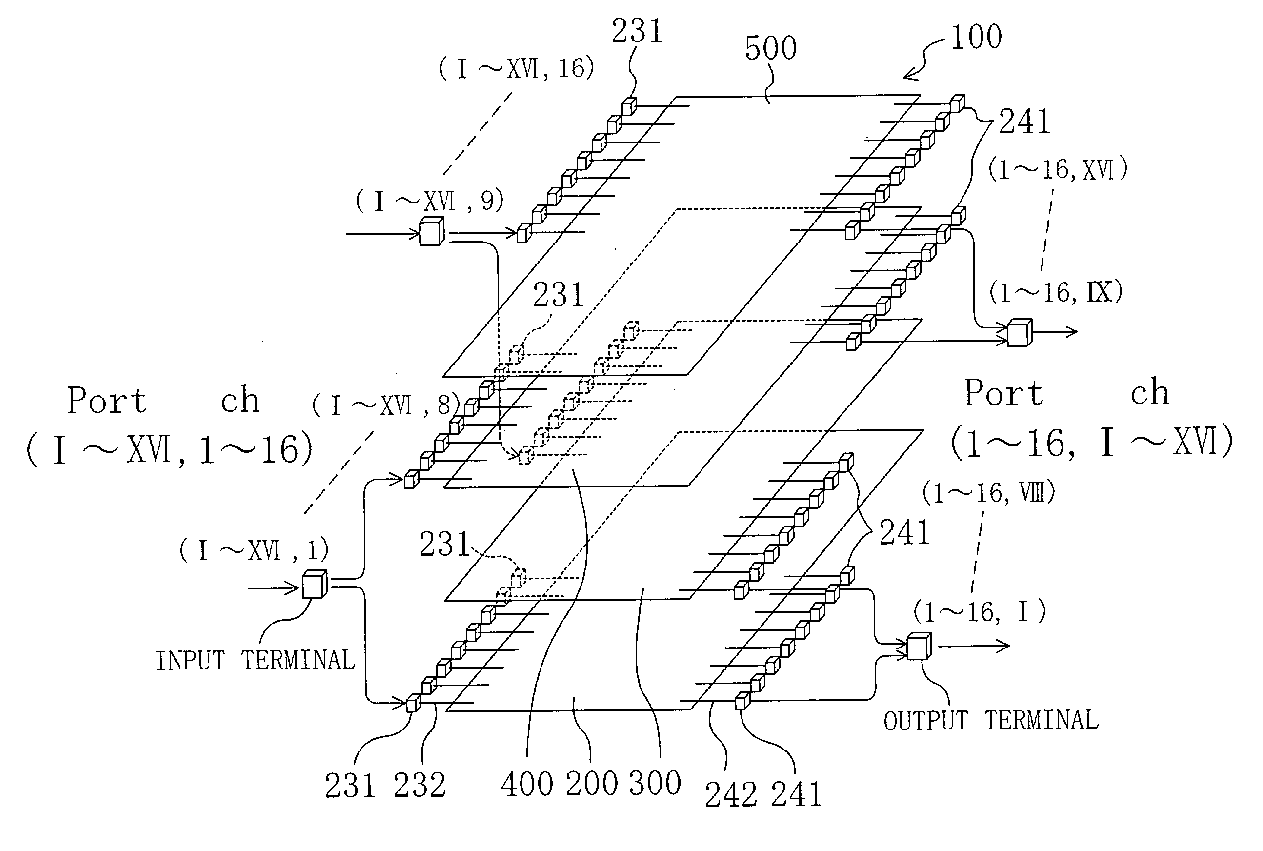
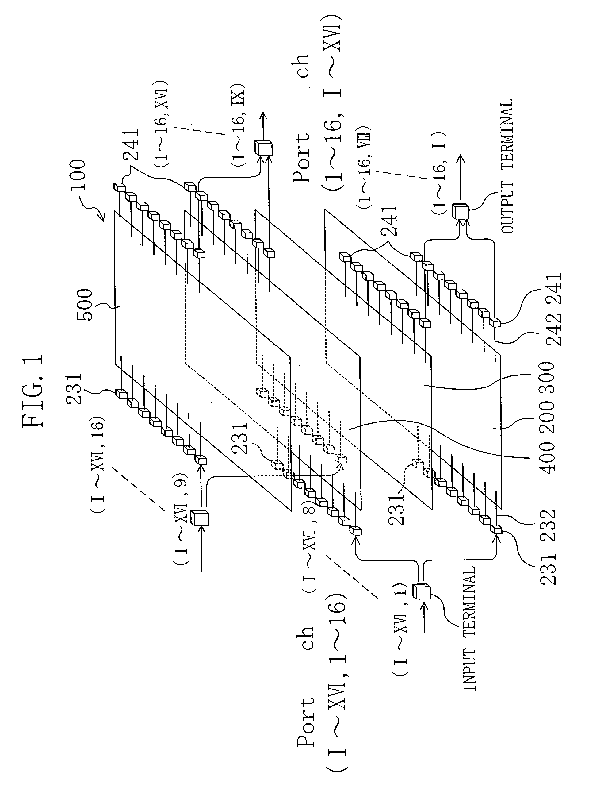
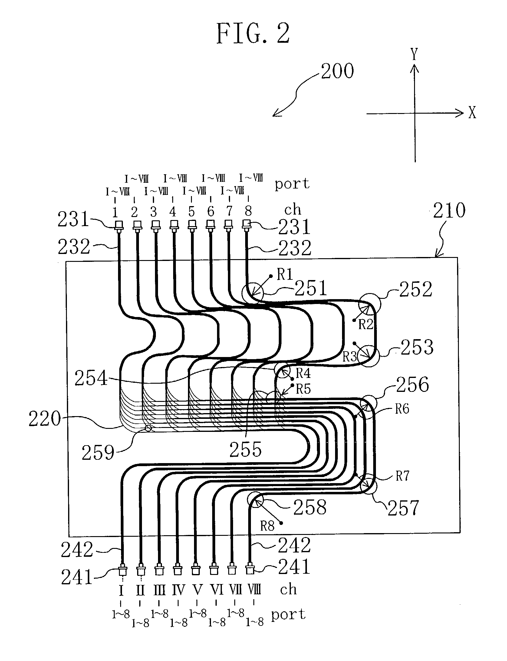
 Specifically, the theoretical cut-off wavelength .lambda.c may be set to be greater than the propagation-light wavelength so that the deviation between the theoretical cut-off wavelength .lambda.c and the propagation-light wavelength is 0.5 .mu.m or less. More specifically, the theoretical cut-off wavelength .lambda.c may be set to satisfy:
.lambda.
[0071] where the propagation-light wavelength is represented by .lambda. [.mu.m].
[0072] Design of the optical fiber 220 will now be described in detail with reference to FIG. 4. An optical fiber used as a reference is an ordinary communication-dedicated single mode optical fiber of which the propagation-light wavelength is 1.55 .mu.m. The relative refraction index difference .DELTA. of this optical fiber is 0.36%, and the core diameter thereof is 8 .mu.m (see arrow a in FIG. 4), whereby the cut-off wavelength .lambda.c is set about 1.28 .mu.m, and the MFD is set about 10.2 .mu.m.
[0073] First, only the relative refraction index difference .DELTA. is increased to 0.38%. Thereby, the MFD is reduced to be slightly less than 10 .mu.m (see arrow b in the same figure). In this state, since the loss of connection to an ordinary communication-dedicated optical fiber is increased, the MFD needs to be increased to an ordinary MFD. Specifically, the core diameter is increased to, for example, 9 .mu.m, whereby the MFD is changed to 10.2 .mu.m (see arrow c in the same figure) so as to become substantially the same as the ordinary MFD.
[0074] At this time, the cut-off wavelength .lambda.c is about 1.48 .mu.m, which is less than the propagation-light wavelength, and the optical fiber can be used as an optical fiber of a 1.55 .mu.m band.
[0075] FIG. 5 shows examples of fiber parameters of an optical fiber to which the present invention is applied. Specifically, in a case where the relative refraction index difference .DELTA. is set to 0.39% and the core diameter is set to 9.3 .mu.m, an optical fiber having a cut-off wavelength .lambda.c of 1.55 .mu.m and an MFD of 10.5 .mu.m can be obtained (Embodiment 1). In addition, in a case where the relative refraction index difference .DELTA. is set to 0.425% and the core diameter is set to 8.8 .mu.m, an optical fiber having a cut-off wavelength .lambda.c of 1.54 .mu.m and an MFD of 10.0 .mu.m can be obtained (Embodiment 2). In the cases of optical fibers to which the present invention is applied, the relative refraction index differences .DELTA. are 0.36% to 0.45%, and the core diameters are 7 .mu.m to 10 .mu.m.
[0076] Generally, the less the relative refraction index difference .DELTA. and the smaller the core diameter of an optical fiber, the more likely the bending loss of the optical fiber occurs. However, in the case of the optical fiber according to the present invention, the absence of consideration of the dispersion enables design to be performed at a degree of freedom increased thereby. Specifically, increasing the relative refraction index difference .DELTA. of the optical fiber enables the bending loss thereof to be reduced. In other words, this enables a reduction in the minimum radius of curvature formed when routing the optical fiber. Accordingly, using the optical fiber enables the minimum radius of curvature (Ra) in the crossover section 259 of each of the sub-wiring boards 200 to 500 to be reduced, and concurrently enabling reduction of each of the radii of curvature (R1 to R8) in the curved portions 251 to 258 (see FIGS. 2 and 3). This enables the sizes of the sub-wiring boards 200 to 500 to be miniaturized, consequently resulting in miniaturization of the size of the optical matrix conversion wiring board 100. In addition, the fiber-routing pattern of the optical fibers on the optical matrix conversion wiring board 100 can be changed to a more intricate fiber-routing pattern. Further, the reduction in the bending loss of the optical fiber 220 enables the performance of the optical matrix conversion wiring board 100 to be stabilized.
[0077] Furthermore, even when the relative refraction index difference .DELTA. is large, the MFD of the optical fiber 220 is substantially the same as the ordinary MFD. This enables the prevention of increase in connection loss occurring when ordinary communication-dedicated optical fibers are connected to the individual input and output ports of the optical matrix conversion wiring board 100.
[0078] It is noted that the optical fiber according to the present invention, that is, the optical fiber of which the bending loss is reduced and the MFD is set to be substantially the same as that of an ordinary communication-dedicated single mode optical fiber, can suitably be used not only for optical-fiber wiring boards, but also for other use environments including many portions where the fiber is bent.

PUM

no PUM

Description & Claims & Application Information

We can also present the details of the Description, Claims and Application information to help users get a comprehensive understanding of the technical details of the patent, such as background art, summary of invention, brief description of drawings, description of embodiments, and other original content. On the other hand, users can also determine the specific scope of protection of the technology through the list of claims; as well as understand the changes in the life cycle of the technology with the presentation of the patent timeline. Login to view more.

Similar technology patents

Three-dimensional integrated circuit cooling system

ActiveUS20180190618A1Increase efficiencyStabilize performanceSemiconductor/solid-state device detailsSolid-state devicesEngineeringThree-dimensional integrated circuit
Owner:MICROJET TECH

Non-Aqueous Electrolyte Solution For Lithium Secondary Battery And Lithium Secondary Battery Including The Same

PendingUS20220131192A1Increase suppressionStabilize performanceLi-accumulatorsOrganic electrolytesAqueous electrolyteOrganosolv
Owner:LG ENERGY SOLUTION LTD

Fuel cell

InactiveUS20090081504A1Stabilize performanceWater management in fuel cellsSolid electrolyte fuel cellsFuel supplyEngineering
Owner:KK TOSHIBA

Classification and recommendation of technical efficacy words

  • Stabilize performance
  • Secure performance

Pneumatic tire

ActiveUS20120285592A1Stabilize performanceTyre tread bands/patternsNon-skid devicesEngineeringGround contact
Owner:YOKOHAMA RUBBER CO LTD

Air-cooling heat dissipation device and system

ActiveUS20180146573A1Increase heat dissipation efficiencyStabilize performanceDigital data processing detailsFlexible member pumpsAirflowEngineering
Owner:MICROJET TECH

Polyethersulfone filtration membrane

InactiveUS20150054197A1Reduction in susceptibilityStabilize performanceSemi-permeable membranesCeramic shaping apparatusBiophysicsPolyether sulphone
Owner:PRESIDENT & FELLOWS OF HARVARD COLLEGE

Air-cooling heat dissipation device

ActiveUS20180240733A1Increase heat dissipation efficiencyStabilize performanceDigital data processing detailsSemiconductor/solid-state device detailsEngineeringAir cooling
Owner:MICROJET TECH

Lens Driving Device, Camera Module and Optical Apparatus

ActiveUS20160291285A1Minimize oscillation phenomenonSecure performanceProjector focusing arrangementNon-rotating vibration suppressionCamera lensFist
Owner:LG INNOTEK CO LTD

Tread Kerf of Snow Tire

InactiveUS20160052346A1Secure performanceTyre tread bands/patternsNon-skid devicesEngineeringWear resistance
Owner:HANKOOK TIRE WORLDWIDE

Folding method of far-side airbag apparatus

ActiveUS20200047705A1Secure performanceDeployment be securedPedestrian/occupant safety arrangementAirbag deploymentStructural engineering
Owner:HYUNDAI MOBIS CO LTD
Why Eureka
Try Eureka