Technique to manufacture a CIS module

Inactive Publication Date: 2003-10-16
YEN YUNG CHAU
View PDF1 Cites 12 Cited by
  • Summary
  • Abstract
  • Description
  • Claims
  • Application Information

AI Technical Summary

Benefits of technology

0008] It is the first object of this invention to provide a technique to elim

Problems solved by technology

It can be seen that there are several drawbacks of the current CIS module manufacturing technique, including
(1) it is difficult to align IC chips to achieve a straight line of linear sensor array,
(2) it is difficult

Method used


Image

  • Technique to manufacture a CIS module
  • Technique to manufacture a CIS module
  • Technique to manufacture a CIS module

Examples


Embodiment Construction

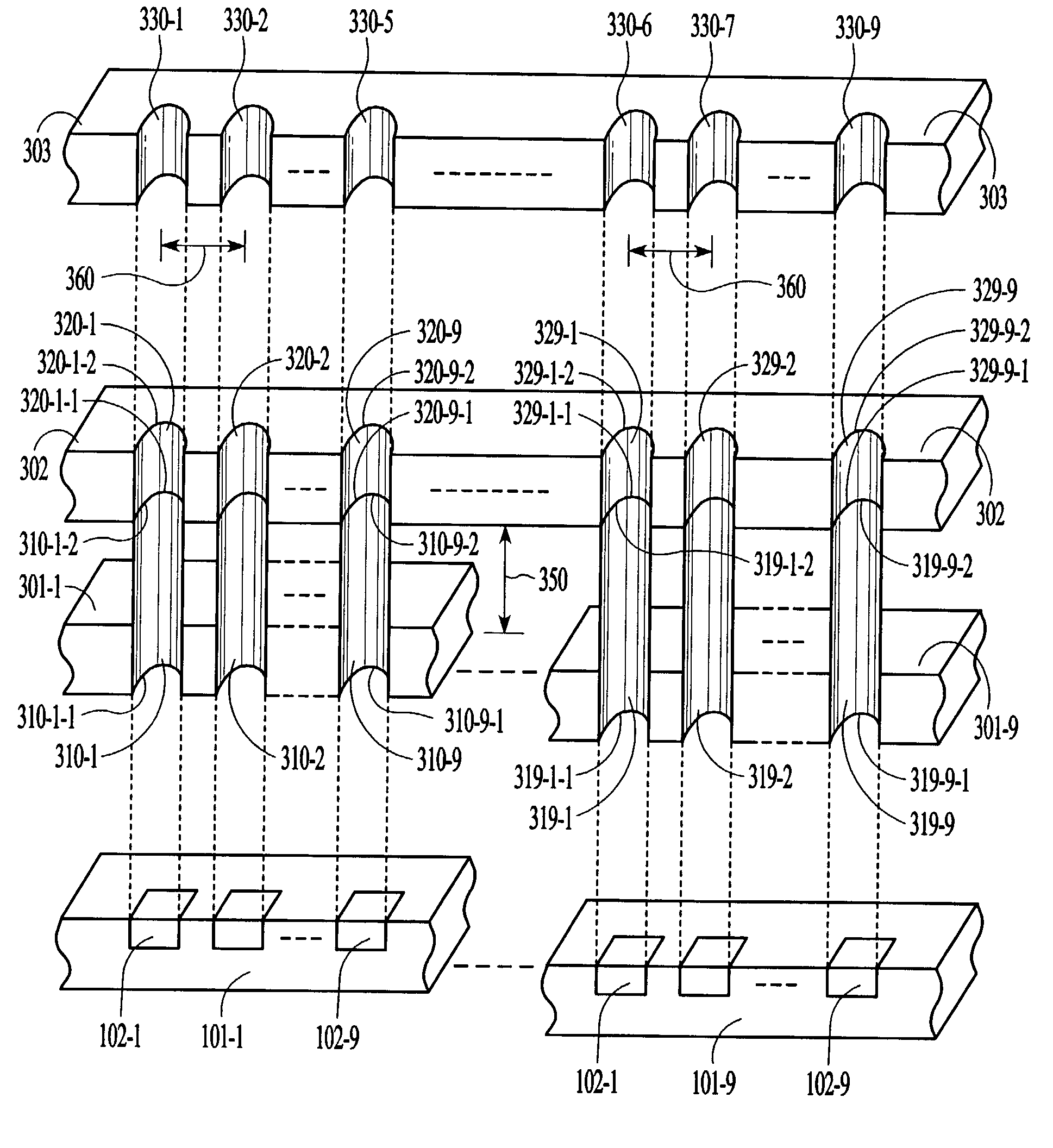
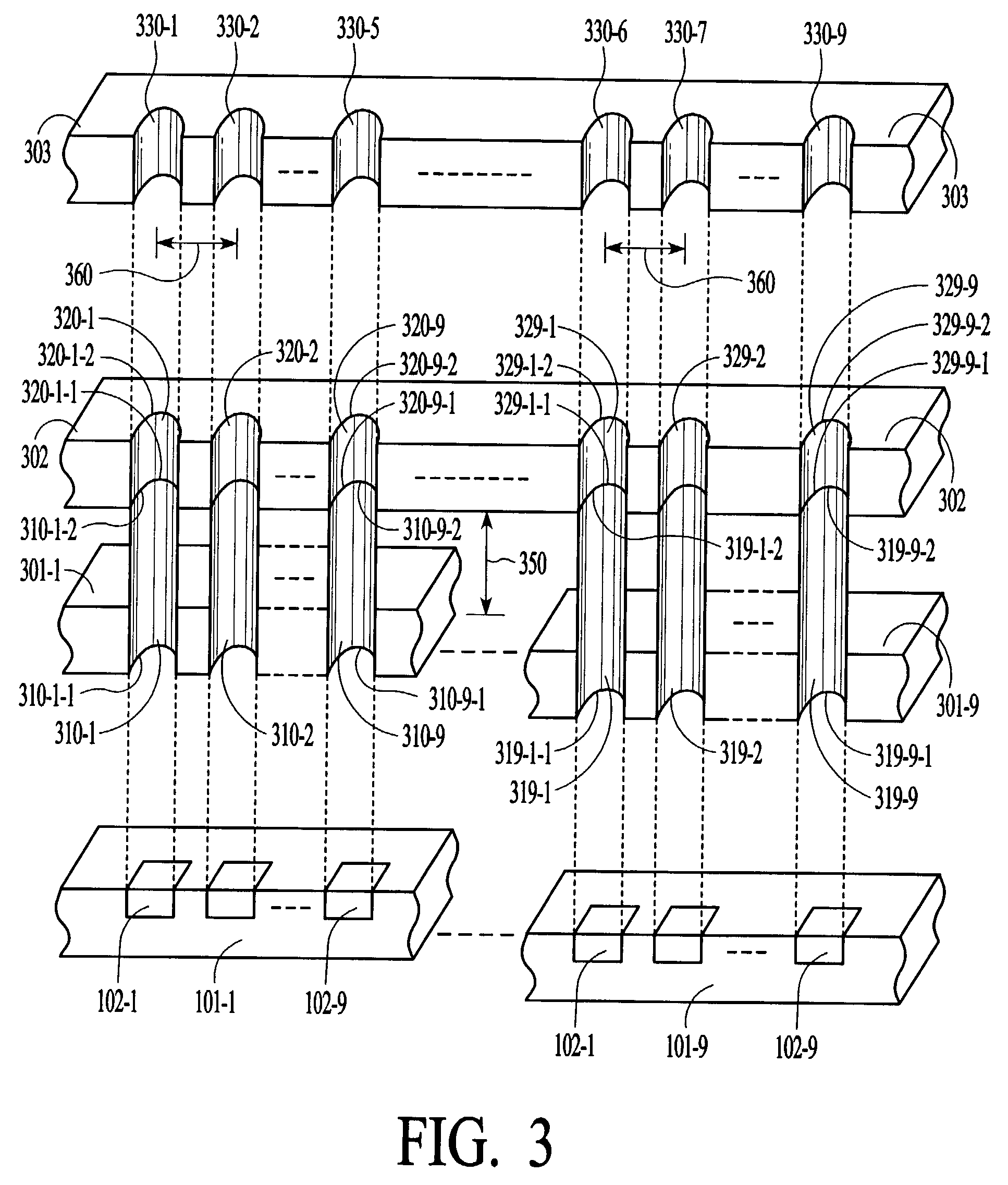
[0023] The fundamental operational principle of this invention to improve CIS module assembly is to employ alignment plate, light-guide plate and resolution plate so that the use of rod lens can be avoided. All alignment plate, light-guide plate and resolution plate are made with a material which is light non-transmissible except light-through structures in alignment plate, light-guide structures in light-guide plate and resolution definition structures in resolution plate. The configuration of three components is in such a manner that alignment plate is between sensor IC chip and light-guide plate which is between alignment plate and resolution plate which is between light-guide plate and line image which consists of a desired number of discrete images which are to be detected by a photo-sensing elements in a linear sensor array. Now, refereeing to FIG. 3, a linear sensor array is formed with a series of sensor arrays of photo-sensing elements from the first sensor array of first p...


PUM


Abstract

A new technique is provided to manufacture a CIS module by employing an alignment-plate, a light-guide plate, and a resolution plate. The above plates can be selected to be pre-fabricated into one piece to reduce the number of components for the CIS module. The dimension of resolution definition structures of resolution plate determines the resolution of CIS module and allows only the reflect light from the image with a desired resolution to pass through. Consequently, it alleviates the butting difficulty in the convention butting operation to form a linear sensor array. Also, a signal reading technique is provided to improve the photo-response of the conventional photo-sensing device. Therefore, operation speed is increased and product performance is improved.

Description

[0001] This invention relates to the field of the image sensing technology, particularly in a CIS (Contact Image Sensor) module manufacturing technique, including a technique to improve butting operation in CIS assembly and a technique to enhance reading photo-response of a photo-sensing element.PRIOR TECHNIQUE[0002] Conventional CIS (Contact Image Sensor) module had the key components which were assembled as shown in FIG. 1 in a cross sectional view in the direction which was perpendicular to the length of the CIS module. On a PCB (Printed Circuits Board) substrate 100, there was a sensor chip array which was formed by butting IC (Integrated Circuits) sensor chip 101 to a desired length along the direction of the CIS module length. Consequently, the sensor chip array formed a linear sensor array to the desired full CIS module length. Each IC sensor chip 101 had the sensor array 102 which comprised of a series of photo-sensing elements. Conventionally, each of photo-sensing elements...

Claims


Application Information

Patent Timeline
IPC IPC(8): H01L27/146H04N1/031H04N5/217
CPCH01L27/14625H01L27/14678H04N1/0318H04N5/357H04N2201/02487H04N2201/03112H04N2201/03129H04N2201/03145H04N2201/03187H04N25/60
Inventor YEN, YUNG CHAU
Owner YEN YUNG CHAU
Why Eureka
Try Eureka