
Virtual ground nonvolatile semiconductor memory array architecture and integrated circuit structure therefor

a virtual ground and memory array technology, applied in static storage, digital storage, instruments, etc., can solve the problems of difficult simultaneous multiple byte programming and page mode programming, and the decoding circuits of source and drain are extremely complex

Inactive Publication Date: 2003-11-27
WINBOND ELECTRONICS CORP
View PDF11 Cites 41 Cited by
  • Summary
  • Abstract
  • Description
  • Claims
  • Application Information

AI Technical Summary

Problems solved by technology

However, simultaneous multiple byte programming and page mode programming are still difficult to achieve.
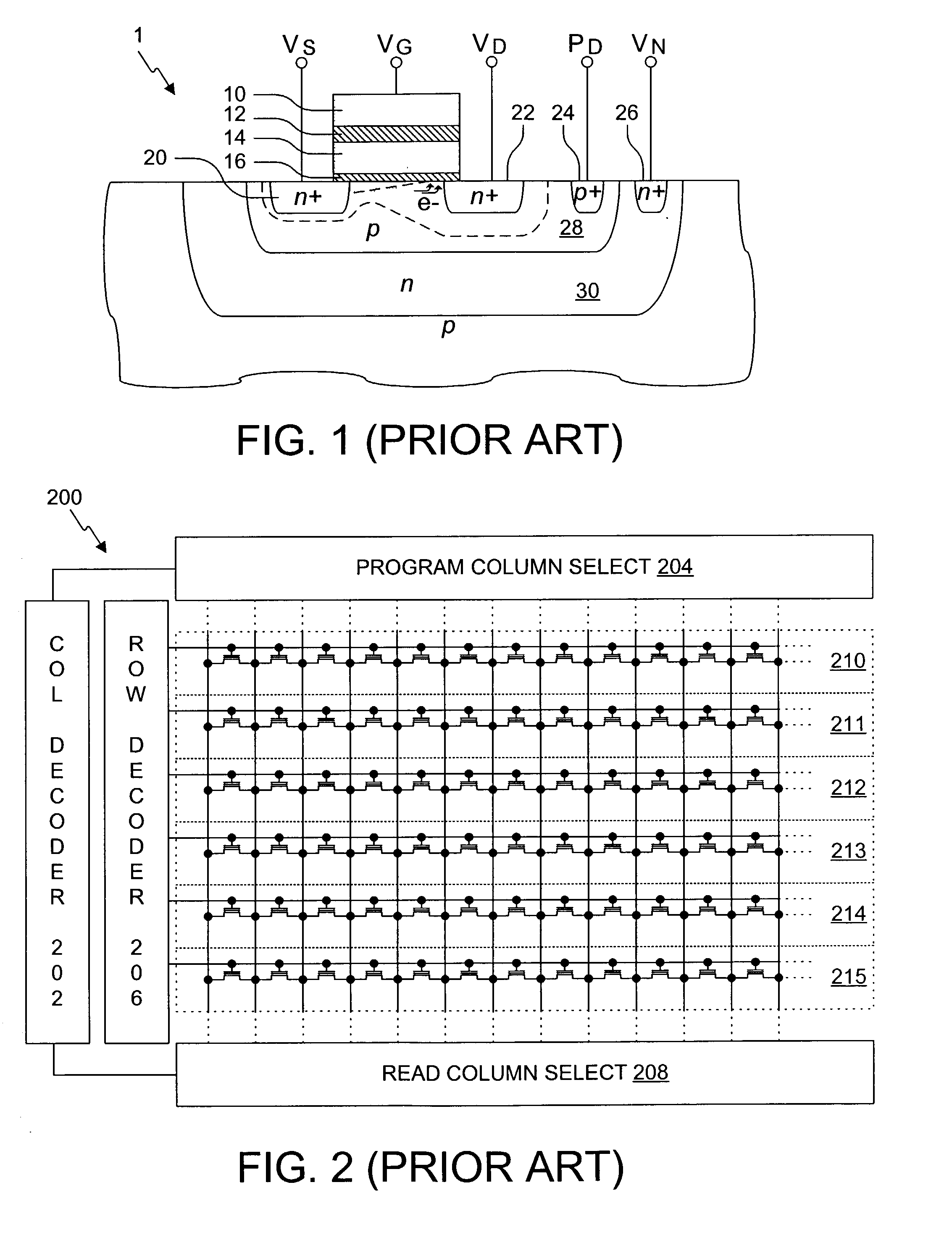
Unfortunately, as in the case the CHE memory array, the use of isolating select transistors in CISEI memory cells increases their size, and the technique of repeated programming groups of bits until the desired amount of memory is programmed can cause program-disturb.
Unfortunately, source and drain decoding circuits tend to be extremely complex because of both the need to use a counterbiasing scheme to reduce voltage disturb on cells sharing the same bit line cell and on cells on other word lines, as well as the large number of decoding combinations necessary for a typical sector of memory.

Method used


Image

  • Virtual ground nonvolatile semiconductor memory array architecture and integrated circuit structure therefor
  • Virtual ground nonvolatile semiconductor memory array architecture and integrated circuit structure therefor
  • Virtual ground nonvolatile semiconductor memory array architecture and integrated circuit structure therefor

Examples


Embodiment Construction

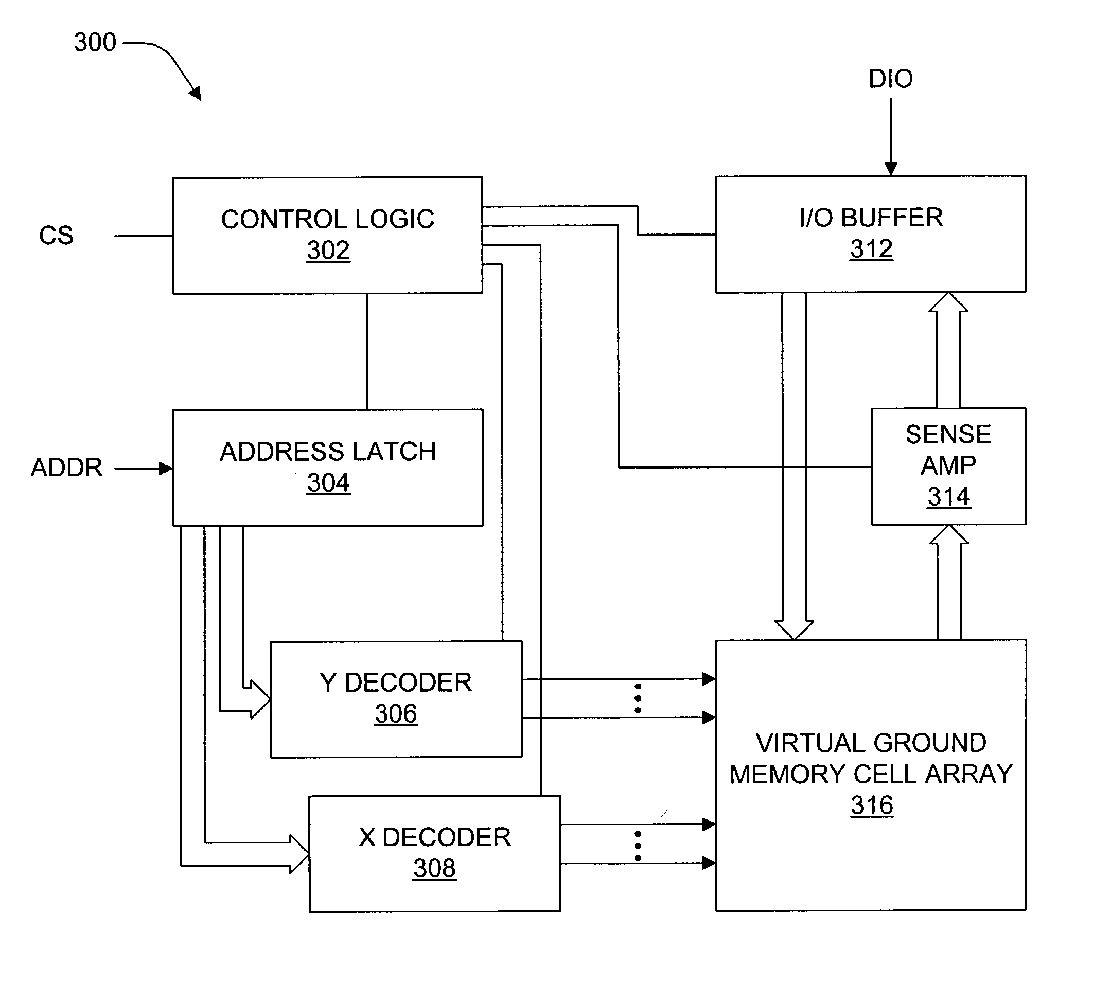
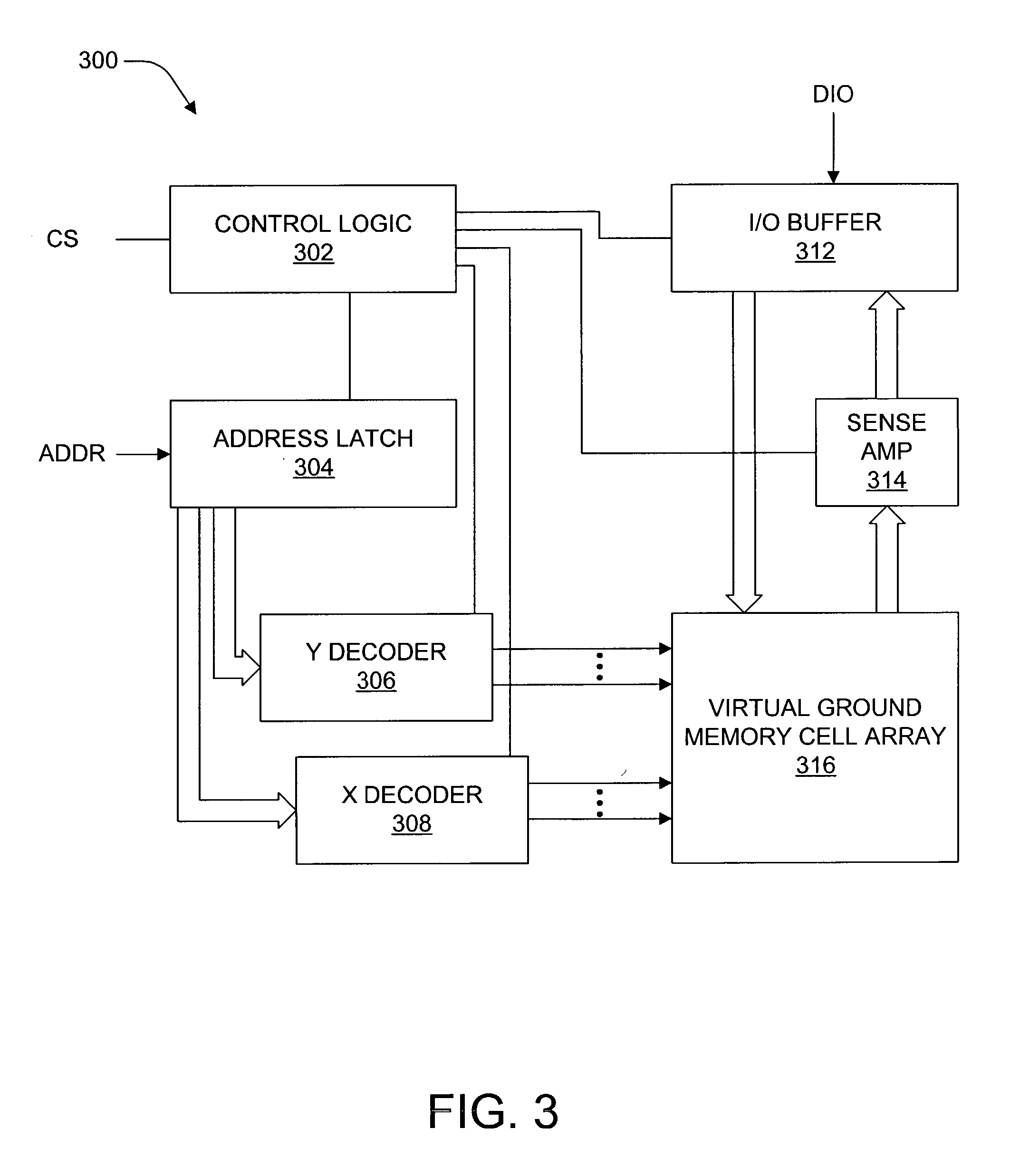
[0036] In an array of nonvolatile memory cells, the memory cells of each sector are organized into groups of successive cells associated with respective groups of successive column lines, the groups of memory cells preferably being of the same size and being isolated from one another by a suitable isolation structure, illustratively oxide formed by any suitable process such as trench isolation or grown field oxide isolation. Because of cell group isolation, each group of column lines may be decoded by its own relatively small program column select, which preferably is replicated in essentially identical form for all groups of column lines. While each program column select preferably is used to decode one group of column lines, larger program column selects may be used if desired to decode two or more groups of column lines. Read column selects may decode one or more groups of column lines as desired, with the number of column lines decoded by the read column selects being the same a...


PUM


Abstract

In nonvolatile memory cell array, the memory cells of each sector are organized into groups of successive cells, the groups preferably being of the same size and preferably isolated from one another in both the row and column directions by a suitable isolation structure such as field dielectric or trench dielectric. Because of cell group isolation, each group of column lines may be decoded by its own relatively small program column select, which preferably is replicated in essentially identical form for all groups of column lines. While each program column select preferably is used to decode one group of column lines, larger program column selects may be used if desired to decode two or more groups of column lines. Read column selects may decode one or more groups of column lines as desired. The number of column lines decoded may the same as or different than the number of column lines decoded.

Description

[0001] 1. Field of the Invention[0002] The present invention relates to semiconductor memory, and more particularly to a nonvolatile virtual ground memory array and method of operation thereof to avoid cell disturb.[0003] 2. Description of the Related Art[0004] Nonvolatile memory retains stored data when power is removed, which is required or at least highly desirable in many different types of computers and other electronic devices. Nonvolatile semiconductor memory devices are generally divided into two main classes. The first class is based on the storage of charge in discrete trapping centers of a dielectric layer of the structure. The second class is based on the storage of charge on a conducting or semiconducting layer that is completely surrounded by a dielectric, typically an oxide.[0005] A common type of stored charge device is the stacked gate transistor, also known as a floating gate transistor, in which cell programming is performed through channel hot-electron injection ...

Claims


Application Information

Patent Timeline
IPC IPC(8): G11C16/04G11C16/08
CPCG11C16/08G11C16/0491
Inventor PARK, JOO WEONHAN, KYUNG JOONKWON, GYU-WANLEE, JONG SEUK
Owner WINBOND ELECTRONICS CORP
Learn More