Transceiver circuit arrangement and method

a technology of transceiver circuit and circuit arrangement, applied in the direction of transmission, electrical equipment, etc., can solve the problems of consuming dc power for switches, vidmar article explains how to perform the necessary functions in a manner suited to low cost and low power radios

Active Publication Date: 2003-11-27
APPLE INC
View PDF8 Cites 33 Cited by
  • Summary
  • Abstract
  • Description
  • Claims
  • Application Information

AI Technical Summary

Problems solved by technology

However, these switches consume an large amount of DC power.
However, such GaAs MESFET switches are typically too expensive.
It may also be a problem with such GaAs MESFET switches to provide enough power handling capability: a 1W signal has a 20V peak-to-peak swing across 50 ohms, thus requiring the FET switch supply to be at least 20V.

Method used


Image

  • Transceiver circuit arrangement and method
  • Transceiver circuit arrangement and method
  • Transceiver circuit arrangement and method

Examples


Embodiment Construction

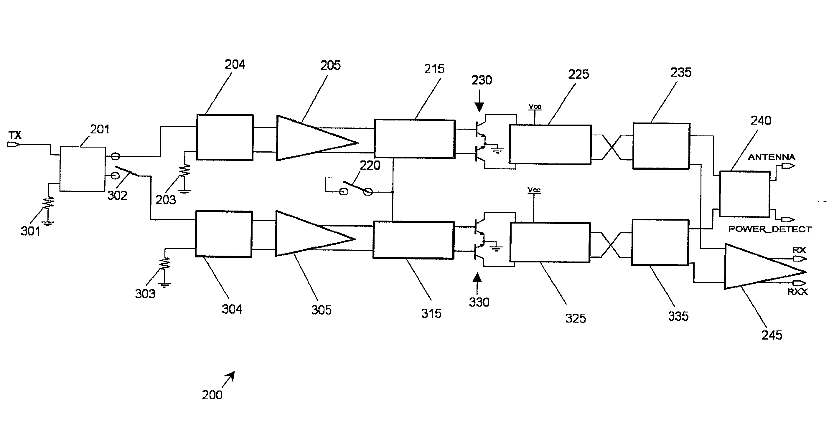
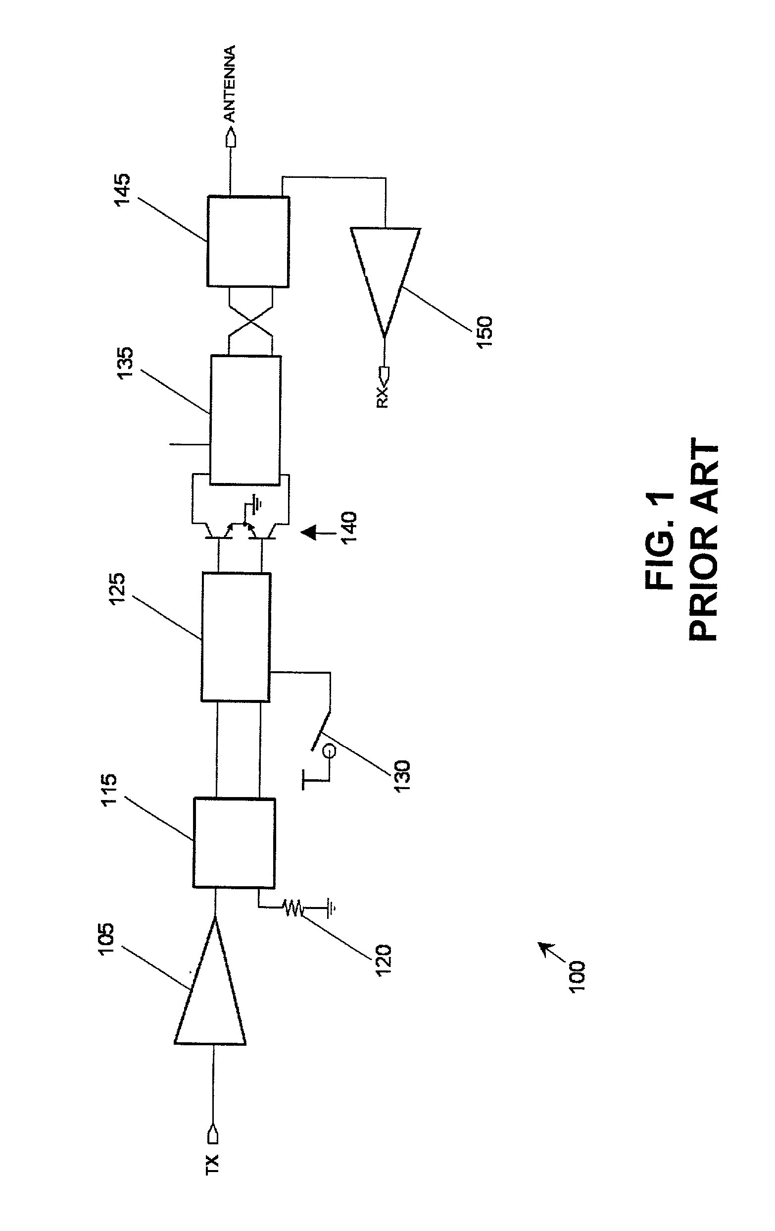
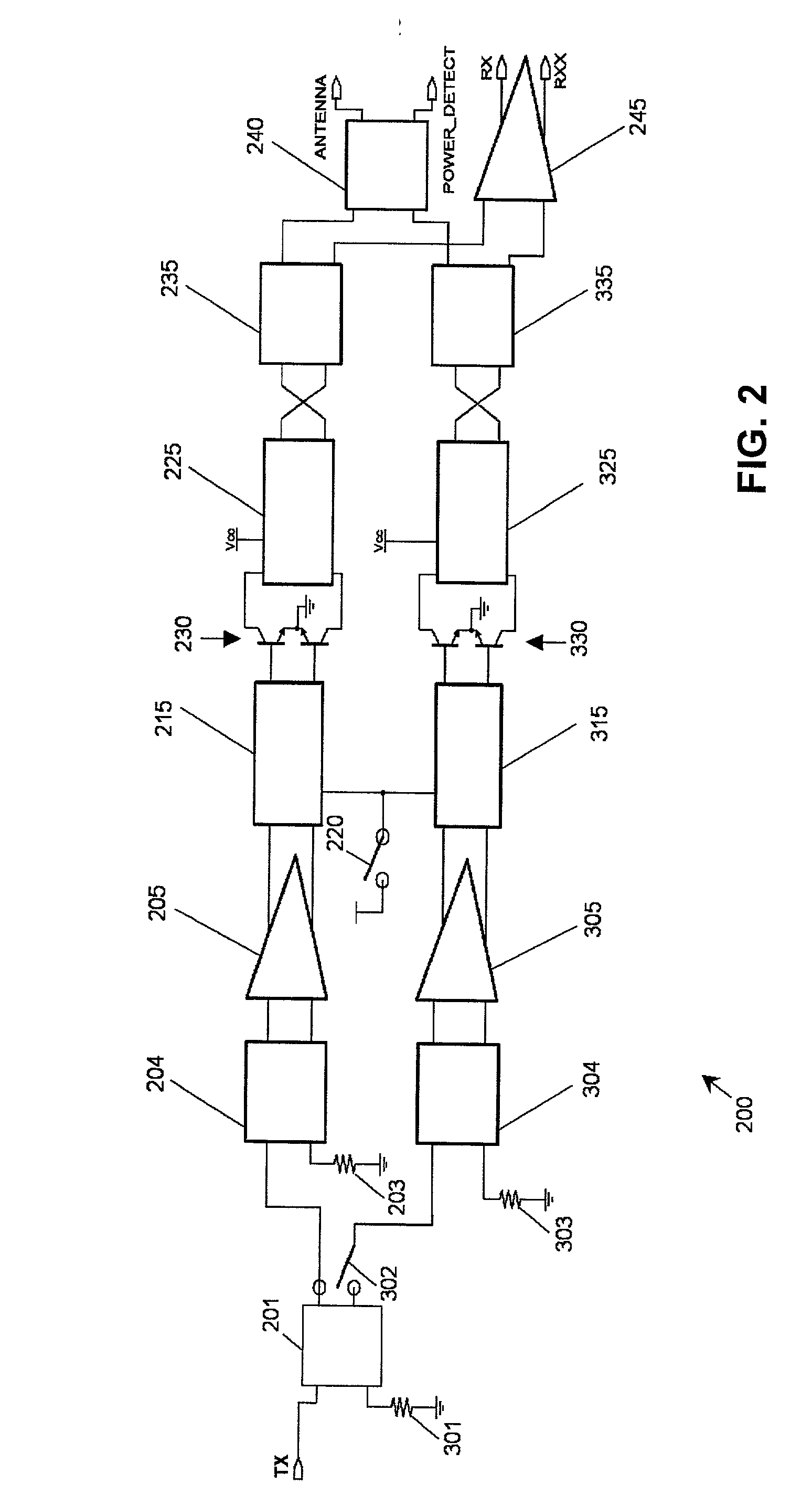
[0012] Referring firstly to FIG. 1, a prior art transceiver circuit 100, for example known from the article by Vidmar, in MICROWAVES & RF, JULY 2000, "Use Transmitting Power FETs for Antenna Switching", includes a terminal TX for receiving a signal for transmission at a radio antenna. The terminal TX is coupled to the input of a driver amplifier 105. The output of the power amplifier 105 is coupled to an input of a 90.degree. hybrid device 115, of which another input is coupled to a resistor 120. The balanced output of the 90.degree. hybrid device 115 is coupled to a bias and matching circuit 125, which is coupled to receive an input voltage dependent on the state of a TX / RX control switch 130. The balanced output of the bias circuit 125 is coupled to a further bias and matching circuit 135 via power transistors 140. The balanced output of the bias circuit 135 is coupled to a 90.degree. hybrid device 145. One output of the 90.degree. hybrid device 145 is connected to a radio antenna...


PUM


Abstract

A doubly balanced transceiver system having a transmit terminal (TX), a receive terminal (RX), and an an antenna terminal (ANTENNA), 180° hybrids (201, 240), 90° hybrids (204, 304, 235 and 335), a power amplifier (230, 330) and a RX/TX switch (220) for disabling the power amplifier so that signals received at the transmitter are reflected to the receive terminal (RX). The 180° hybrids (201, 240) preferably split and re-combine signals into parallel paths. A loopback test mode is preferably provided by use of an antenna isolation switch (302) to enable a power detect terminal (POWER_DETECT). This eliminates pricey and problematic GaAs switches, and allows the use of low cost silicon for the power amplifier. The doubly balance architecture also has the advantage of eliminating common-mode noise, and reflection problems with the PA gain stages. Additionally, greater power can be extracted from the power amplifier. Further the arrangement has less insertion loss compared to a GaAs switch. Also, dependant upon system specifications, it may be possible to eliminate harmonic filtering at the power amplifier output.

Description

[0001] This invention relates to radio frequency electronic circuits, and particularly, though not exclusively, to such circuits for use in wireless data transceiver applications.[0002] In the field of wireless data transceiver circuits it is known that prior solutions have used a PIN diode and quarter-wavelength transmission lines as a switch between transmit and receive. Such a prior art solution is known, for example, from U.S. Pat. No. 4,701,724 "Injection Switch and Directional Coupler". However, these switches consume an large amount of DC power.[0003] It is also known to use GaAs MESFETs to form a single-pole, double-throw switch. However, such GaAs MESFET switches are typically too expensive. It may also be a problem with such GaAs MESFET switches to provide enough power handling capability: a 1W signal has a 20V peak-to-peak swing across 50 ohms, thus requiring the FET switch supply to be at least 20V.[0004] From U.S. Pat. No. 5,606,283 "Monolithic Multi-Function Balanced S...

Claims


Application Information

Patent Timeline
IPC IPC(8): H04B1/52
CPCH04B1/52
Inventor DYKSTRA, JEFFREY A.TANZI, NEBIL
Owner APPLE INC
Why Eureka
Try Eureka