Field emission display device

a field emission display and field emission technology, applied in the direction of discharge tube main electrodes, discharge tube luminescnet screens, discharge tube with screens, etc., can solve the problems of reducing the performance and lifetime of the emitter, poor mechanical properties of the emitter, and large work functions of metals or semi-conductive materials used for the emitter

Inactive Publication Date: 2004-01-15
HON HAI PRECISION IND CO LTD
View PDF6 Cites 10 Cited by
  • Summary
  • Abstract
  • Description
  • Claims
  • Application Information

AI Technical Summary

Benefits of technology

[0007] In view of the above-described problems of the related art, an object of the present invention is to provide a field emission display (FED) device with nano-scale electron emitters having low emitting voltage and excellent mechanical properties.

Problems solved by technology

One major problem of the conventional FED device is that the work functions of metals or semiconductive materials used for the emitters are large.
Another major problem is the poor mechanical properties of the emitters.
These problems reduce the performance and lifetime of the emitters.
The electrons extracted from the outermost layer of the cathode cause non-uniform electron emission, and therefore non-uniform brightness at the phosphors.

Method used


Image

  • Field emission display device
  • Field emission display device

Examples


Embodiment Construction

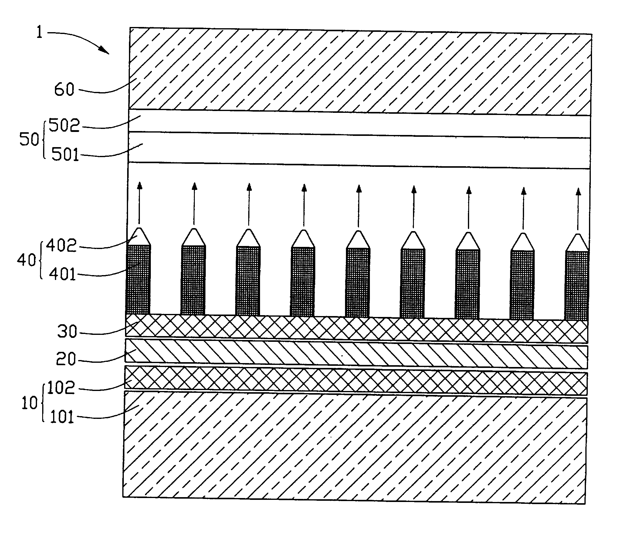
[0013] Referring to FIG. 1, a field emission display device 1 in accordance with a preferred embodiment of the present invention comprises a first substrate 10, a cathode plate 20 made from electrically conductive material formed on the first substrate 10, a resistive buffer 30 in contact with the cathode plate 20, a plurality of electron emitters 40 formed on the resistive buffer 30, an anode plate 50 spaced from the electron emitters 40 thereby defining an interspace (not labeled) region between the electron emitters 40 and the anode plate 50, and a second substrate 60.

[0014] The first substrate 10 comprises a glass plate 101 and a silicon thin film 102. The silicon thin film 102 is formed on the glass plate 101 for providing effective contact between the glass plate 101 and the cathode plate 20.

[0015] Each of the electron emitters 40 comprises a nano-rod first part 401 formed on the buffer 30 and a conical second part 402 formed on a free end of respective nano-rod 401. The buffe...


PUM


Abstract

A field emission display device (1) includes a cathode plate (20), a resistive buffer (30) in contact with the cathode plate, a plurality of electron emitters (40) formed on the buffer, and an anode plate (50) spaced from the electron emitters. Each electron emitter includes a nano-rod first part (401) and a conical second part (402). The buffer and the nano-rods are made from silicon carbide (SiCX). The combined buffer and nano-rods has a gradient distribution of electrical resistivity such that highest electrical resistivity is nearest the cathode plate and lowest electrical resistivity is nearest-the anode plate. The conical parts are made from molybdenum. When emitting voltage is applied between the cathode and anode plates, electrons emitted from the electron emitters traverse the interspace region and are received by the anode plate. Because of the gradient distribution of electrical resistivity, only a very low emitting voltage is needed.

Description

[0001] 1. Field of the Invention[0002] The present invention relates to a field emission display (FED) device, and more particularly to an FED device using nano-scale electron emitters having low emitting voltage and excellent mechanical properties.[0003] 2. Description of Related Art[0004] In a conventional FED device, electrons are extracted from emitters on a cathode by applying an emitting voltage to tips of the emitters. The emitters are made of metals such as molybdenum, or semiconductive materials such as silicon. The electrons impinge on phosphors on the back of a transparent cover plate and thereby produce an image.[0005] One major problem of the conventional FED device is that the work functions of metals or semiconductive materials used for the emitters are large. That is, the emitting voltage required for electron emission is very high. Another major problem is the poor mechanical properties of the emitters. When residual gas particles in a vacuum within the FED device c...

Claims


Application Information

Patent Timeline
Patent Type & Authority Applications(United States)
IPC IPC(8): H01J1/02H01J1/30H01J1/304H01J1/62H01J19/24H01J29/04H01J31/12
CPCH01J1/3044Y10S977/952H01J2329/00
Inventor CHEN, GA-LANE
Owner HON HAI PRECISION IND CO LTD
Why Eureka
Try Eureka