Semiconductor device and method of manufacturing same

Active Publication Date: 2004-02-26
RENESAS ELECTRONICS CORP
View PDF1 Cites 18 Cited by
  • Summary
  • Abstract
  • Description
  • Claims
  • Application Information

AI Technical Summary

Benefits of technology

[0014] A second object of the present invention is to provide a semiconductor device in which the side wall surface of an interconnect interlayer film will not sustain damage, and to a method of manufacturing this device.
[0016] According to a first aspect of the present invention, the foregoing object is attained by providing a method of manufacturing a semiconductor device that forms a dual damascene interconnect structure. The method comprises the steps of: forming at least a light absorbing sacrificial film, which has an etching rate different from that of a photoresist and is capable of being removed using a stripping solution, on a semiconductor substrate so as to embed the film in a trench pattern in such a manner that the overall surface of the film will be flat, wherein the semiconductor substrate has been obtained by forming at least a first interlayer film, an etching stopper film, a second interlayer film, a first hard mask and a second hard mask on a substrate in the order mentioned, the second hard mask being formed to have the trench pattern, which exposes the first hard mask. The method further comprises: forming the photoresist on the light absorbing sacrificial film, the photoresist having an aperture pattern, which is disposed over the area of the trench pattern, having an opening width less than that of the trench pattern; and selectively etching, one after the other, at least the light absorbing sacrificial film, the first hard mask and the second interlayer film using the photoresist as an etching mask. In accordance with this structure, the surface of the light absorbing sacrificial film that is exposed from the opening in the photoresist is flattened and a satisfactory selection ratio is obtained between the photoresist and the light absorbing sacrificial film. As a result, the opening width of the opening in the photoresist is stabilized at the time of etching and a dual damascene interconnect structure having an excellent precision-worked shape is obtained.
[0017] According to a second aspect of the present invention, the foregoing object is attained by providing a method of manufacturing a semiconductor device that forms a dual damascene interconnect structure. The method comprises the steps of: forming at least a sacrificial film, which has an etching rate different from that of a photoresist and is capable of being removed using a stripping solution, on a semiconductor substrate so as to embed the film in a trench pattern in such a manner that the overall surface of the film will be flat, wherein the semiconductor substrate has been obtained by forming at least a first interlayer film, an etching stopper film, a second interlayer film, a first hard mask and a second hard mask on a substrate in the order mentioned, the second hard mask being formed to have the trench pattern, which exposes the first hard mask; forming an anti-reflective film on the sacrificial film. The method further comprises: forming the photoresist on the anti-reflective film, the photoresist having an aperture pattern, which is disposed over the area of the trench pattern, having an opening width less than that of the trench pattern; and selectively etching, one after the other, at least the anti-reflective film, the sacrificial film, the first hard mask and the second interlayer film using the photoresist as an etching mask. In accordance with this structure, the surface of the anti-reflective film that is exposed from the opening in the photoresist is flattened and the anti-reflective film can be reduced to a constant thickness. As a result, retraction of the opening in the photoresist is suppressed at the time of etching and dual damascene interconnect structure having an excellent precision-worked shape is obtained.
[0019] According to a fourth aspect of the present invention, the foregoing object is attained by providing a method of manufacturing a semiconductor device that forms a dual damascene interconnect structure. The method comprises the steps of: forming at least a sacrificial film, which has an etching rate different from that of a photoresist and is capable of being removed using a stripping solution, on a semiconductor substrate so as to embed the film in a trench pattern in such a manner that the overall surface of the film will be flat, wherein the semiconductor substrate has been obtained by forming at least a cap film, a first interlayer film, an etching stopper film, a second interlayer film and a hard mask on a substrate in the order mentioned, the hard mask and the second interlayer film being formed to have the trench pattern, which exposes the etching stopper film. The method further comprises: forming an anti-reflective film on the sacrificial film; forming the photoresist on the anti-reflective film, the photoresist having an aperture pattern, which is disposed over the area of the trench pattern, having an opening width less than that of the trench pattern; and selectively etching, one after the other, at least the anti-reflective film, the sacrificial film, the etching stopper film and the first interlayer film using the photoresist as an etching mask. In accordance with this structure, the surface of the anti-reflective film that is exposed from the opening in the photoresist is flattened and the anti-reflective film can be reduced to a constant thickness. As a result, retraction of the opening in the photoresist is suppressed at the time of etching and deep trench can be formed.

Problems solved by technology

The conventional method relying upon dual hard masks is such that it is difficult to obtain an excellent precision-worked shape for a dual damascene interconnect structure.
The result is an interconnect having an unacceptable (unstable) shape (see FIG. 6B).

Method used


Image

  • Semiconductor device and method of manufacturing same
  • Semiconductor device and method of manufacturing same
  • Semiconductor device and method of manufacturing same

Examples


first embodiment

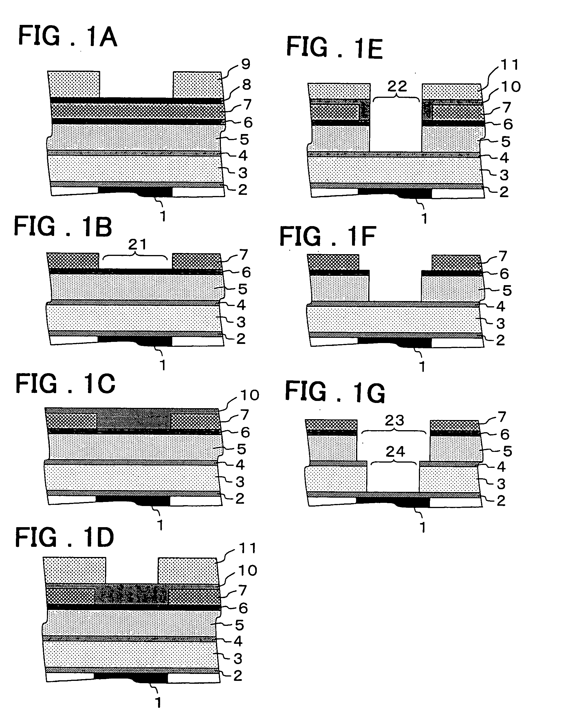
[0043] FIGS. 1A-1G are partial sectional views schematically illustrating a substrate at each step of a method of manufacturing a semiconductor device according to the present invention.

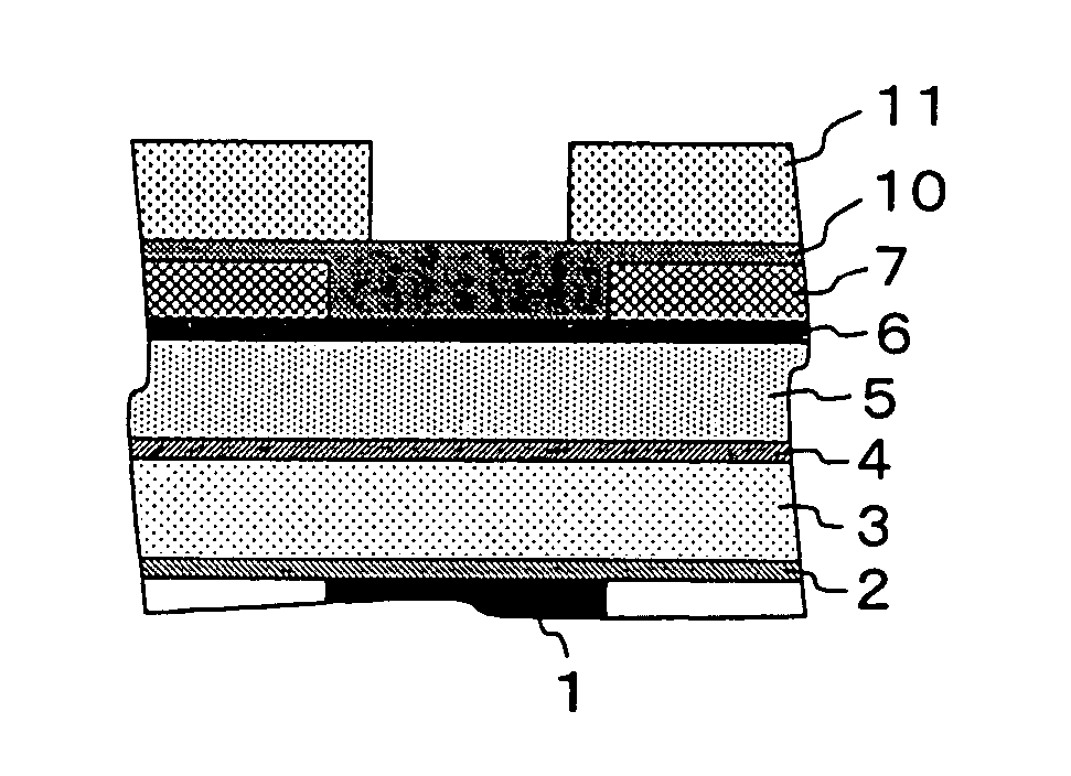
[0044] First, films are formed on the surface of a substrate on which has been formed the Cu bottom-layer interconnect layer 1, which is exposed at the surface. Specifically, through use of CVD (Chemical Vapor Deposition) or coating method, the cap film 2 (SiCN having a film thickness of 50 nm), the via interlayer film 3 (SiOC having a film thickness of 350 to 400 nm), the etching stopper film 4 (SiC having a film thickness of 50 nm), the interconnect interlayer film 5 (SiOC having a film thickness of 300 nm), the first hard mask 6 (SiO.sub.2 having a film thickness of 500 nm) and the second hard mask 7 (SiN having a film thickness of 1500 nm) are formed on the surface of the substrate in the order mentioned [step A1; see FIG. 1A].

[0045] Next, the anti-reflective film 8 (organic BARC having a film th...

second embodiment

[0051] the present invention will now be described.

[0052] The method of the second embodiment is almost the same as the method of manufacturing a semiconductor device according to the first embodiment but differs in that an organic polymer is used for the via interlayer film 3 and interconnect interlayer film 5 (see FIG. 1). The MSQ-based light absorbing sacrificial film 10 is such that a satisfactory selection ratio is obtained relative to the organic polymer as well. Even if the etching at step A4 [see FIG. 1E] in the first embodiment is carried out, therefore, the organic polymer of the interconnect interlayer film 5 can be etched while the dimensions of the MSQ-based light absorbing sacrificial film 10 are maintained in excellent fashion. This makes it possible to obtain an excellent precision-worked shape. The etching here also is carried out while successively adjusting the etching gases such as C.sub.xF.sub.y, C.sub.xH.sub.yF.sub.z, Ar, N.sub.2, O.sub.2, etc., in such a manne...

third embodiment

[0053] the present invention will now be described.

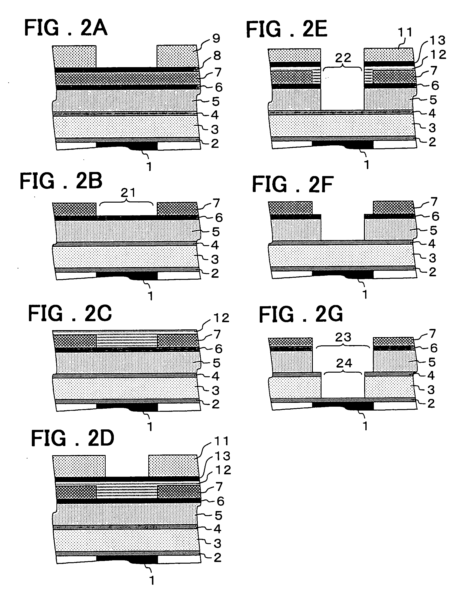
[0054] FIG. 2 is a partial sectional view schematically illustrating a substrate at each step of a method of manufacturing a semiconductor device according to a third embodiment of the present invention.

[0055] First, films are formed on the surface of a substrate on which has been formed the Cu bottom-layer interconnect layer 1, which is exposed at the surface. Specifically, through use of CVD or a coating method, the cap film 2 (SiCN having a film thickness of 50 nm), the via interlayer film 3 (SiOC having a film thickness of 350 to 400 nm), the etching stopper film 4 (SiC having a film thickness of 50 nm), the interconnect interlayer film 5 (SiOC having a film thickness of 300 nm), the first hard mask 6 (SiO.sub.2 having a film thickness of 500 nm) and the second hard mask 7 (SiN having a film thickness of 1500 nm) are formed on the surface of the substrate in the order mentioned [see FIG. 1A].

[0056] Next, the first anti-reflectiv...


PUM


Abstract

Disclosed is a semiconductor device having a precision-worked dual damascene structure. A semiconductor substrate is obtained by forming at least a first interlayer film, an etching stopper film, a second interlayer film, a first hard mask and a second hard mask on a substrate in the order mentioned, the second hard mask being formed to have a trench pattern. At least a light absorbing sacrificial film, which has an etching rate different from that of a photoresist and is removable by use of a stripping solution, is formed on the semiconductor substrate in such a manner that the overall surface thereof will be flat. The photoresist is formed on the light absorbing sacrificial film and has an aperture pattern whose opening width is less than that of the trench pattern. At least the light absorbing sacrificial film, the first hard mask and the second interlayer film are etched selectively, one after the other, using the photoresist as an etching mask.

Description

[0001] This invention relates to a semiconductor device in which a dual damascene interconnect structure is formed, and to a method of manufacturing the same. More specifically, the invention relates to a semiconductor device having an excellent precision-worked shape, and to a method of manufacturing the same.[0002] An embedded interconnect (damascene) technique is effective as a method of forming multiple-layer interconnects in a semiconductor integrated circuit device. One such technique is a dual damascene technique wherein an interconnect trench in which a top-layer interconnect is formed and a via hole (or contact hole) that connects the top-layer interconnect and a bottom-layer interconnect (or substrate) are formed in an insulating film, after which the same metal film is embedded in the interconnect trench and via hole to form the interconnect and via into a unitary body. The dual damascene technique is advantageous in that manufacturing cost can be reduced greatly owing to...

Claims


Application Information

Patent Timeline
IPC IPC(8): H01L21/4763G03F7/40H01L21/768H01L23/52H01L27/15
CPCH01L21/76808H01L21/76813H01L21/76811
Inventor ARITA, KOJITAGAMI, MASAYOSHIMIYAMOTO, HIDENOBU
Owner RENESAS ELECTRONICS CORP
Why Eureka
Try Eureka