Bending actuators and sensors constructed from shaped active materials and methods for making the same

a technology of actuators and active materials, applied in the field of actuators and sensors, can solve the problems of non-restricted morphs, large actuation travel for a given applied field, and non-uniform piezoelectric activity

Inactive Publication Date: 2004-03-25
MONODRIVE
View PDF15 Cites 43 Cited by
  • Summary
  • Abstract
  • Description
  • Claims
  • Application Information

AI Technical Summary

Benefits of technology

0039] It is yet another object of the present invention to provide a single slab, homogeneous material, bending actuator and bending sensor design for MEMS applications that does not suffer from deposition stress or metallic bonding failures.

Problems solved by technology

Furthermore, morphs are completely unrestrained over at least some large portion of their extent to allow bending.
Field uniformity within each active slab increases the effectiveness of the actuation and hence leads to larger actuation travel for a given applied field.
This non-uniform piezoelectric activity leads to moments when stimulated with a uniform field.
Bonding piezoelectric materials to a metal slab is difficult and, in fact, many morph device failures are attributable to the metal / piezoelectric material interface.
The large stresses inherently present in the active slabs of morphs have other deleterious effects on actuator function.
For example, large stresses contribute to device aging.
In addition, the large internal stresses contribute to material failure.
Thus, single layer, plane parallel homogeneous active member slabs cannot be used independently as bending sensors.
Since the second slab is crucial to the functionality of the device, all the complexities and problems described above in the fabrication and function of morph style actuators are also present in morph style sensors.
The architecture inherent in morph style actuators and sensors is difficult to implement in millimeter and sub millimeter devices.
The difficulties come from using discrete components to obtain the regions of different piezoelectric activity required to make a unimorph or bimorph style device.
The task of assembling individual components becomes burdensome as these discrete components become small and correspondingly delicate.
These deposition processes have associated problems.
The elevated temperatures required during these processing steps lead to large residual stresses due to coefficient of thermal expansion, CTE, mismatches between the various layers required by morphs for actuation.
In addition, film densification causes further shrinkage and leads to more residual stress.
Hence, finished, room temperature devices exhibit large internal stresses, curling and other similar effects.
The CTE mismatch issues remain with the device making the actuator inherently sensitive to temperature changes in the environment.
In addition, as devices get smaller, the thickness of bonding layers and inactive layers, caused by contamination or material composition changes during processing, get relatively bigger, increasingly impacting the efficiency of the device.
For layered MEMS devices, layer to layer bonding failure represents a significant reliability problem.
Another characteristic of sub millimeter devices is that the stiffness or mechanical impedance of the devices diminishes rapidly due to the relationship between stiffness and member thickness.
In addition, it is difficult to find stable, non-active layers of a workable thickness sufficiently compliant relative to the stiffness of the active layer for efficient actuation.
Furthermore, there is a need to reduce the sensitivity of small bender devices to thermal changes.

Method used


Image

  • Bending actuators and sensors constructed from shaped active materials and methods for making the same
  • Bending actuators and sensors constructed from shaped active materials and methods for making the same
  • Bending actuators and sensors constructed from shaped active materials and methods for making the same

Examples


Embodiment Construction

)

[0072] In describing the preferred embodiment of the present invention, reference will be made herein to FIGS. 1-15 of the drawings in which like numerals refer to like features of the invention.

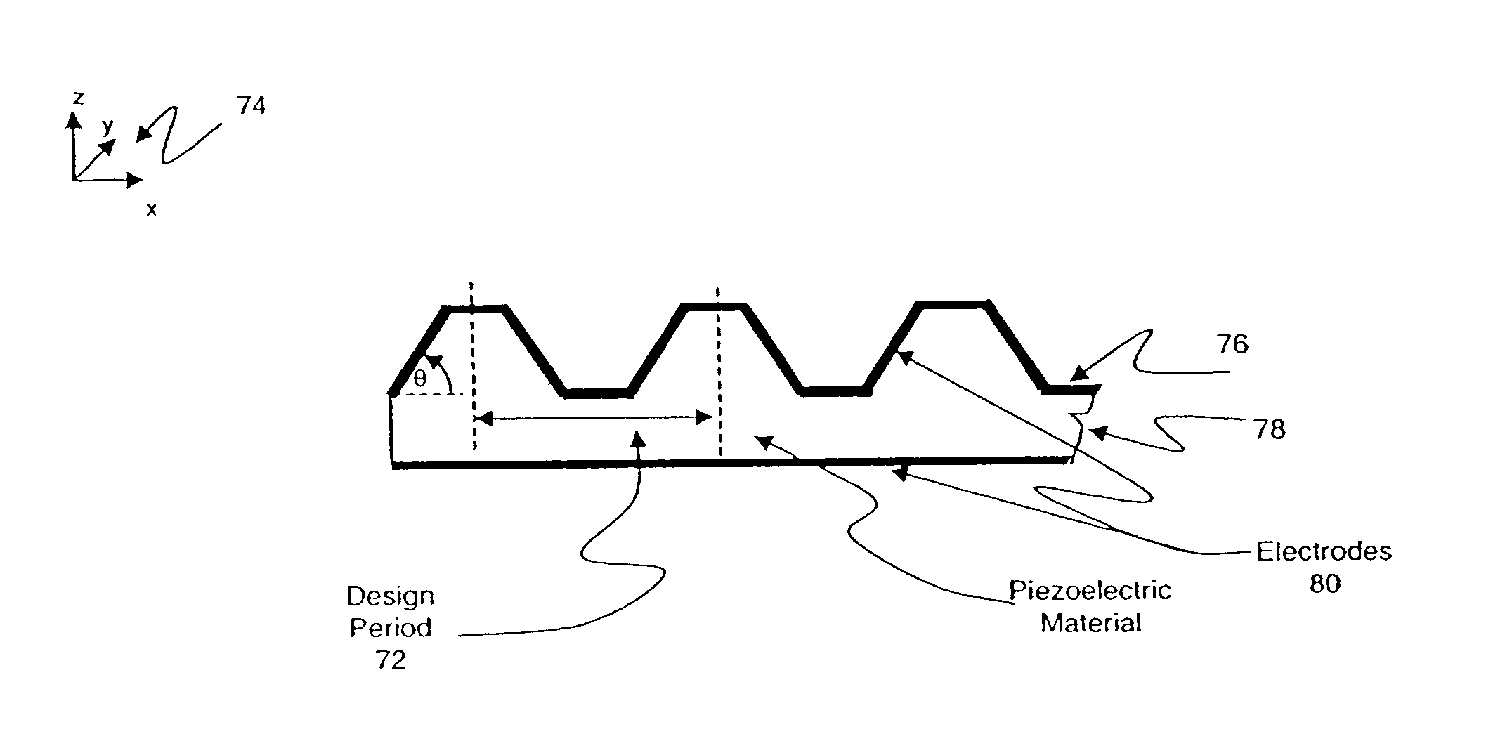
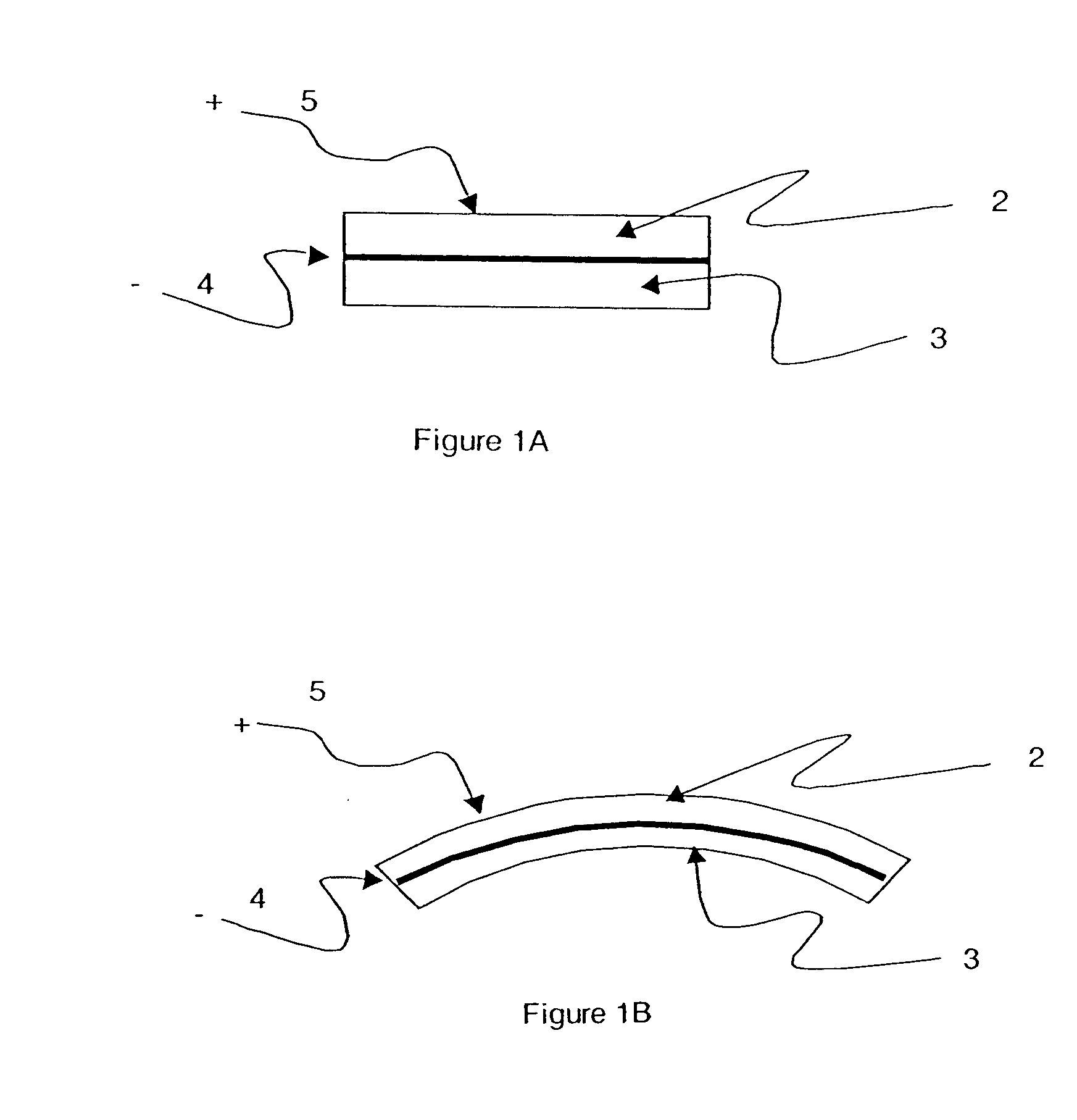
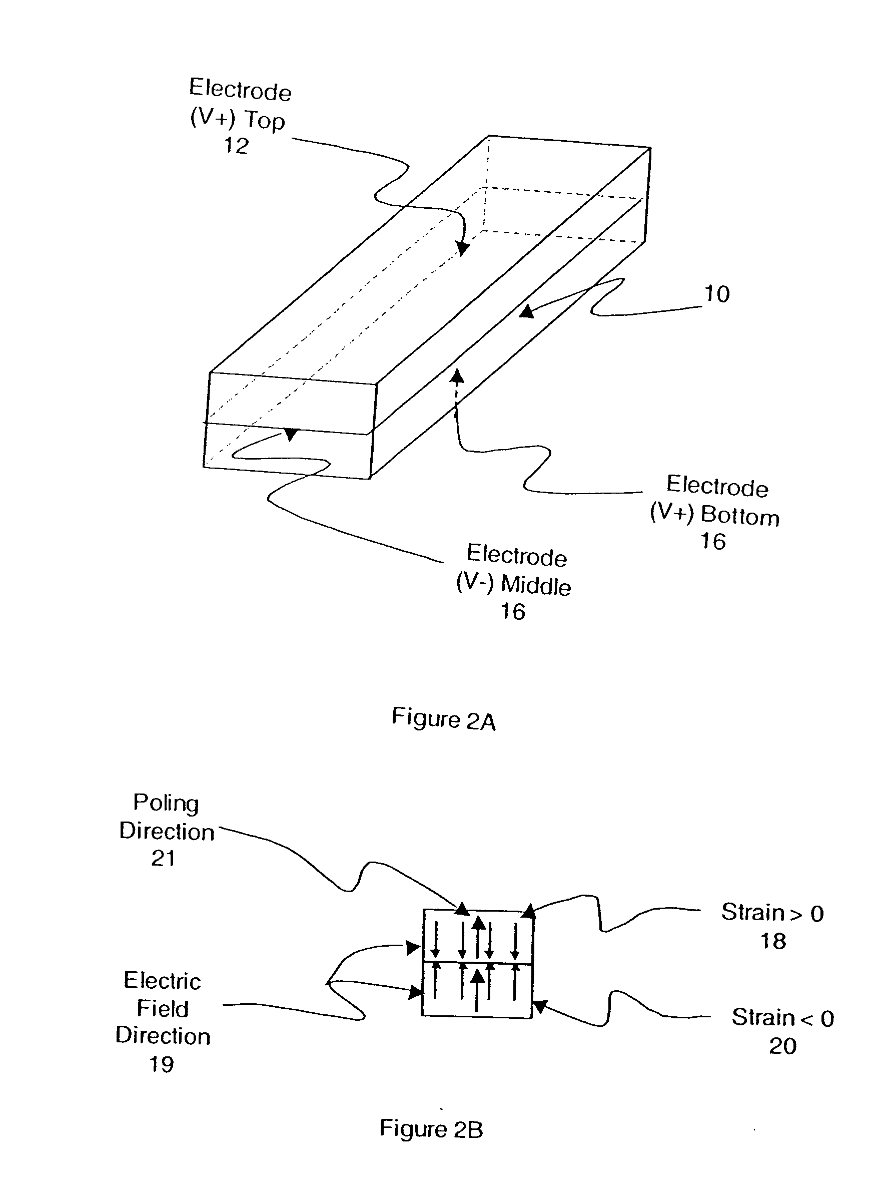
[0073] The present invention relates to the use of active materials for which the physical properties and electromechanical state functions of the material are responsive to applied energy fields. A shaping of the external topology generates within the material non-uniform fields for the express purpose of exploiting the resulting non-uniform distribution of physical properties or the electromechanical state functions established as a result of the external topology for generating moments and bending the member. In one embodiment, an actuator based on bending is presented. The bending is caused by a non-uniform strain-inducing field generated within a single homogeneous slab of a non-planar geometry and non-uniform thickness. In another embodiment, a sensor is presented through the use of a...


PUM


Abstract

Bender devices are demonstrated by developing non-uniform fields within a homogeneous, non-planar single slab active member material of non-uniform thickness through geometrical constraints and electrode placement. Single slab actuators are demonstrated for semiconductor designs including MEMS applications. Single slab bender periodic designs are demonstrated to be well suited for MEMS fabrication. Shaped actuators having a topological pattern formed across at least one portion are demonstrated to induced strain at the patterned portion of the actuator, causing the patterned portion to flare into open and close positions upon application of an external field. Voltage transformers, spark generators, power sources, and sensors are developed using the non-planar, homogeneous, single slab active member material of non-uniform thickness. Last, semiconductor process design techniques are demonstrated for periodic and other non-planar single slab actuators.

Description

[0001] 1. Field of the Invention[0002] The present invention relates to actuators, and sensors, and specifically to bending actuators and sensors. More specifically, the present invention relates to the generation of a non-uniform strain-inducing field within a single slab bending actuator and the generation of asymmetric fields in a bending sensor, having a predetermined geometry and non-uniform thickness.[0003] 2. Description of Related Art[0004] For a large class of materials, the material properties such as strain and stress, and the like, can be changed and controlled by the application of an external energy, typically in the form of a field. Materials that exhibit these effects are considered "active materials." As an example, electric, magnetic, and electromagnetic fields induce changes in physical properties of certain materials. More specifically, the application of an electric field to a piezoelectric material changes the overall shape of the material in known, repeatable ...

Claims


Application Information

Patent Timeline
Patent Type & Authority Applications(United States)
IPC IPC(8): H01L41/09H01L41/107H01L41/113H01L41/12H01L41/24H02N2/00H02N2/18
CPCH01L41/107H01L41/1132H01L41/12H01L41/098H01L41/318H01L41/094H01L41/47H10N30/204H10N30/2048H10N30/40H10N30/302H10N35/00H10N30/081G01L1/22H10N30/078H10N30/2042H10N35/01
Inventor MENZEL, CHRISTOPH P.
Owner MONODRIVE
Why Eureka
Try Eureka