Method for fabricating a through-hole interconnection substrate and a through-hole interconnection substrate

a technology of through-hole interconnection and through-hole interconnection, which is applied in the manufacture of printed circuits, printed electric components, basic electric elements, etc., can solve the problems of high temperature and heat-resistant sheets exceeding the tolerance of heat-resistant sheets, and the inability to fully fill metal in the ends of micro-holes

a technology of through-hole interconnection and through-hole interconnection, which is applied in the manufacture of printed circuits, printed electric components, basic electric elements, etc., can solve the problems of high temperature and heat-resistant sheets exceeding the tolerance of heat-resistant sheets, and the inability to fully fill metal in the ends of micro-holes

US20040092117A1Inactive Publication Date: 2004-05-13THE FUJIKURA CABLE WORKS LTD

Image

  • Method for fabricating a through-hole interconnection substrate and a through-hole interconnection substrate
  • Method for fabricating a through-hole interconnection substrate and a through-hole interconnection substrate
  • Method for fabricating a through-hole interconnection substrate and a through-hole interconnection substrate

Examples


Embodiment Construction

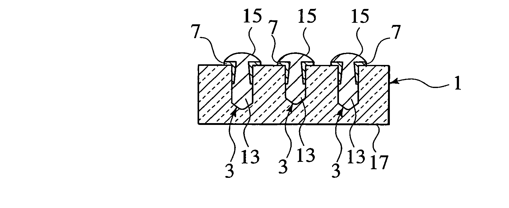
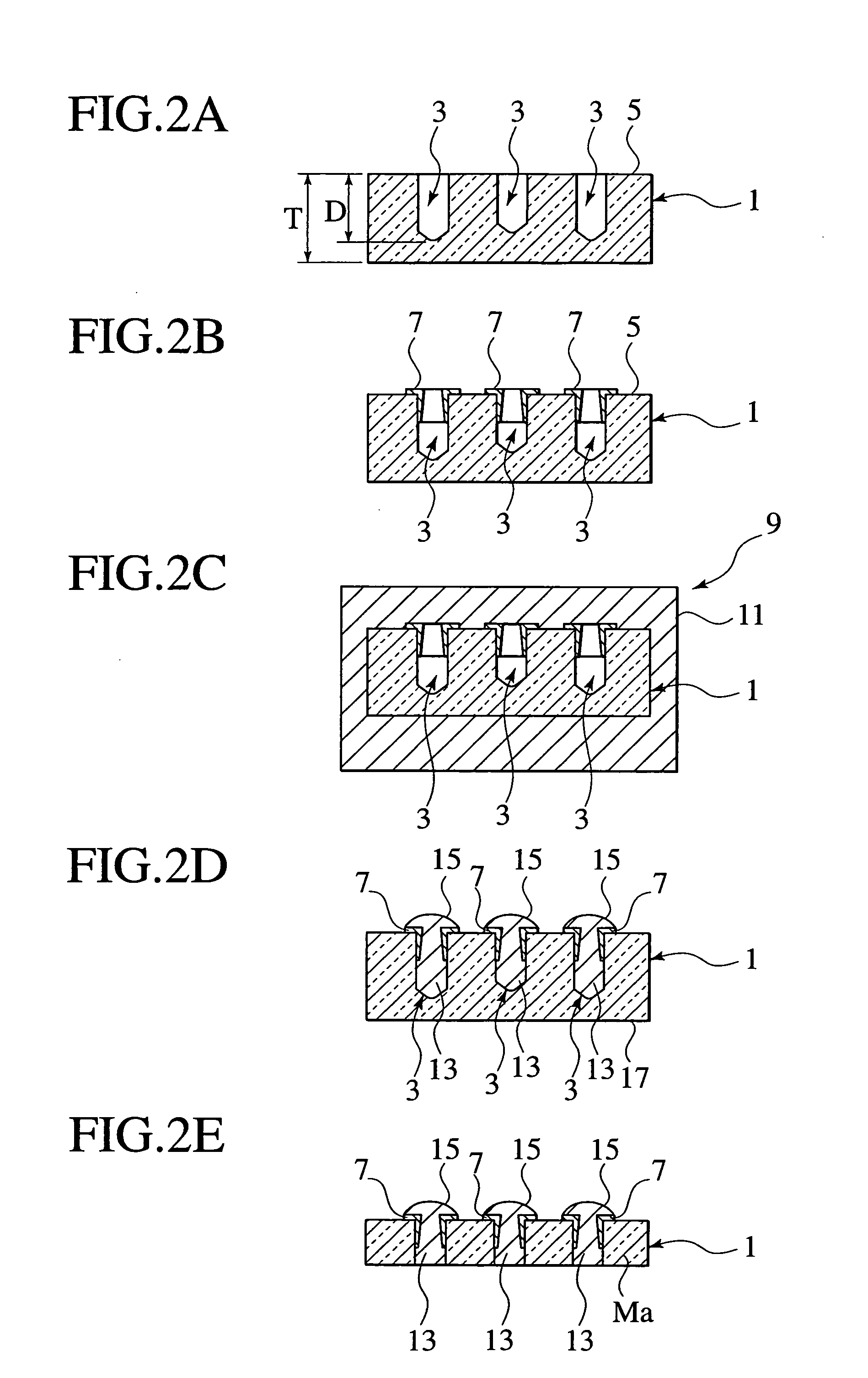
[0022] Exemplary embodiments of the invention will now be described with reference to the accompanying drawings. The described exemplary embodiments are intended to assist the understanding of the invention, and are not intended to limit the scope of the invention in any way.

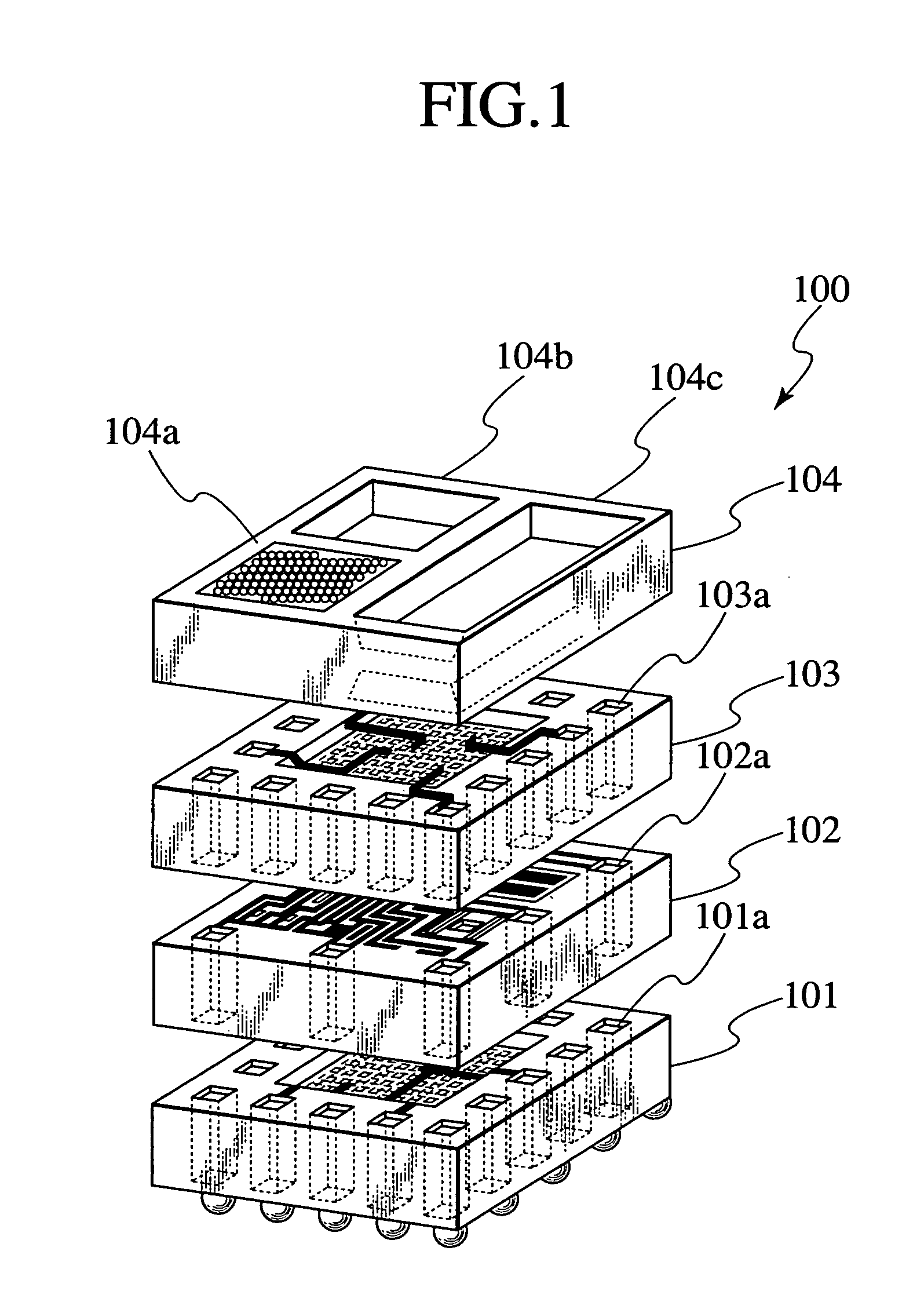
[0023] Referring to FIG. 1, a multilayer device 100 includes IC (Integrated Circuit) chips 101, 102, and 103 as three stacked layers. Multilayer device 100 includes a sensor chip 104 on IC chip 103. IC chips 101, 102, and 103 include through-hole interconnections 101a, 102a, and 103a in peripheral edges thereof, respectively. Through-hole interconnections 101a, 102a and 103a electrically connect IC chips 101, 102 and 103 with each other. Sensor chip 104 includes gas sensor 104a, pressure sensor 104b, and IR sensor 104c on a surface thereoL

[0024] A method for fabricating multilayer device 100 includes the steps of processing a work, forming a circuit pattern, and bonding a wire. The work is processed as below.

[00...


PUM

PropertyMeasurementUnit
Thicknessaaaaaaaaaa
Pressureaaaaaaaaaa
Electrical conductoraaaaaaaaaa

Abstract

A blind hole (3) is formed on a substrate (1) from a first side of the substrate toward a second side of the substrate (1). A conductor (11) is filled in the blind hole (3). The substrate (1) is removed from the opposite side to expose the conductor (13) filled in the blind hole (3).

Description

[0001] This application claims the benefit of Japanese Patent Application P 2002-324135, filed Nov. 7, 2002 in the Japanese Patent Office, the disclosure of which is incorporated herein in its entirety by reference.[0002] 1. Field of the Invention[0003] The present invention relates to a method for fabricating a through-hole interconnection substrate and a through-hole interconnection substrate. More specifically, the present invention is adapted for a high-density three-dimensional packaging of stacking a silicon IC chip and the like or to a contact thereof. The present invention is also adapted for a silicon optical bench for implementing an optical device such as a laser diode, a photodiode and an optical waveguide.[0004] According to the present invention, a metal for a conductor is filled in micro-holes for through-hole electrodes. The through hole electrodes are utilized for interconnecting wiring patterns formed on front and back surfaces of a silicon substrate, to be employe...

Claims


Application Information

Patent Timeline
13 May 2004
Publication
US20040092117A1
IPC
H01L21/288; H01L23/14; H01L21/3063; H01L21/48; H01L21/768; H01L23/48; H01L25/065
CPC
H01L21/288; Y10T29/49117; H01L21/486; H01L21/76898; H01L23/481; H01L25/0657; H01L2924/09701; H05K1/0306
Inventors
SUEMASU, TATSUO; TAKIZAWA, TAKASHI