Automatic material handling system, production system for semiconductor device, and production management method for semiconductor device

Inactive Publication Date: 2004-05-13
SEMICON ENERGY LAB CO LTD
View PDF6 Cites 8 Cited by
  • Summary
  • Abstract
  • Description
  • Claims
  • Application Information

AI Technical Summary

Problems solved by technology

Although an element as the impurity is necessary for forming the source/drain region, the impurity is a contaminant that becomes a cause of chemical contamination against the substrate in the process in a different manufacturing process, and it has an adverse affect on characteristics of the semiconductor device that the substrate is contaminated by the element.
Since the substrate after doping is transferred with the AGV to a manu

Method used


Image

  • Automatic material handling system, production system for semiconductor device, and production management method for semiconductor device
  • Automatic material handling system, production system for semiconductor device, and production management method for semiconductor device
  • Automatic material handling system, production system for semiconductor device, and production management method for semiconductor device

Examples


embodiment

[0121] [Embodiment]

[0122] Hereinafter, an embodiment according to the present invention will be explained.

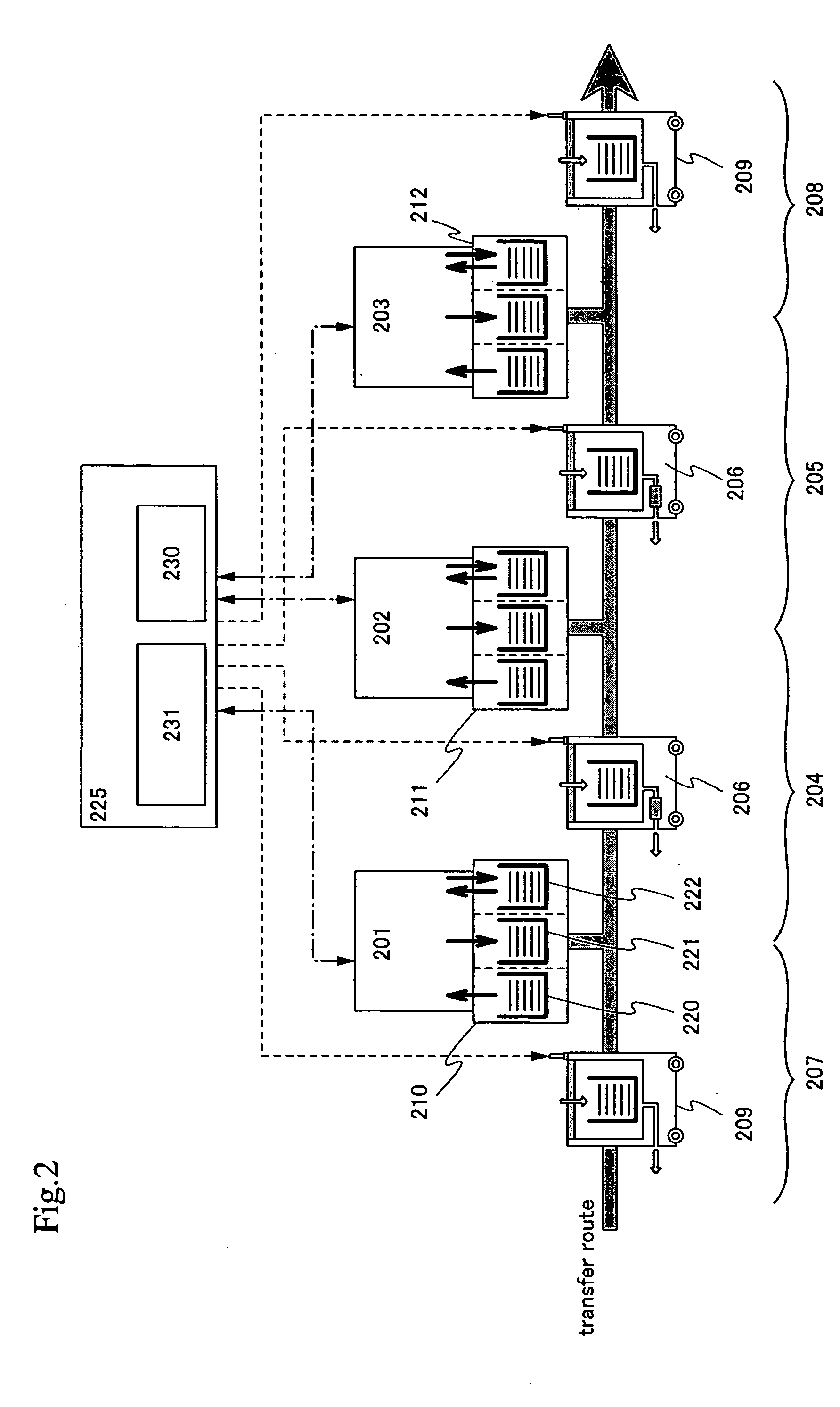
[0123] In the present embodiment mode, an explanation will be given on the content of a process sheet held as data in the memory 230 provided in the host computer 225 in the production system shown in FIG. 2.

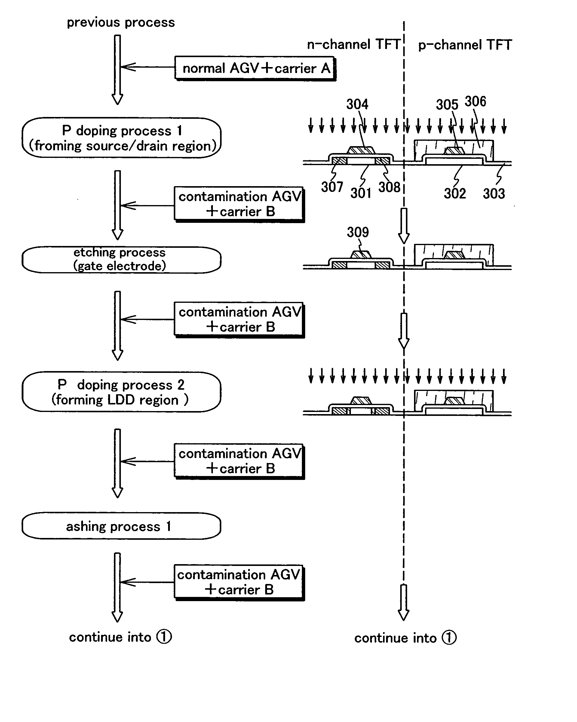
[0124] In the case of controlling a transfer of a carrier with the use of an AGV by the host computer 225 as shown in FIG. 2, the memory 230 has information held as data on transfer routes of the contamination AGV, among all transfer routes of a carrier among plural manufacturing systems, and each of specific manufacturing systems or processes, for which a carrier before processing is changed to another carrier after processing.

[0125] FIG. 9 shows a process sheet for a manufacturing process of a semiconductor device that has an n-channel TFT and a p-channel TFT. In accordance with the process sheet shown in FIG. 9, a carrier is changed in each of manufacturing systems corres...


PUM


Abstract

It is an object to provide an AGV that enables preventing a substrate and a manufacturing system from being contaminated due to another substrate with an adhering contaminant generated in a manufacturing process, and also a production system for a semiconductor device and a production management method for a semiconductor device, which use the AGV. In the present invention, air filtered through a filter is introduced into a containing portion of an AGV, and air in the containing portion containing a carrier is exhausted after filtering the air in the containing portion through another filter. As the filter used before discharging the air, a filter that enables filtering an impurity on the order of a submicron level is used. In addition, a carrier used before doping is changed to another carrier after doping, and CIM system is used to control driving of the AGV and selection of the carrier.

Description

[0001] 1. Field of the Invention[0002] The present invention relates to an auto-guided vehicle (AGV) that transfers a substrate for forming a semiconductor device in a clean room. The present invention also relates to a production system and a production management method for a semiconductor device, for managing a production line that uses the AGV for a semiconductor device[0003] 2. Description of the Related Art[0004] In a production line for a semiconductor device, a cleanliness level required for a clean room is varied depending on a degree of integration. In general, it is considered that a dust with a grain size that is equivalent to one tenth of a design rule or more has an influence on characteristics of a product, and a higher cleanliness level is required for a clean room with a higher degree of integration.[0005] In order to obtain the higher cleanliness level, an AGV that automatically transfers a substrate between manufacturing systems in a clean room. With the automatic...

Claims


Application Information

Patent Timeline
IPC IPC(8): B65G49/00B65G49/07H01L21/00H01L21/02H01L21/677
CPCH01L21/67017H01L21/67724H01L21/67276H01L21/00
Inventor OHTANI, HISASHITSUJI, EIICHIRO
Owner SEMICON ENERGY LAB CO LTD
Why Eureka
Try Eureka