

Interfact circuit
a technology of interface circuit and interface circuit, which is applied in the direction of generating/distributing signals, instruments, liquid/fluent solid measurement, etc., can solve the problems of large power consumption of the master oscillator itself, limitation of efforts to reduce power consumption, and conventional otg capability
- Summary
- Abstract
- Description
- Claims
- Application Information
AI Technical Summary
Benefits of technology
Problems solved by technology
Method used
Image

Examples
first embodiment
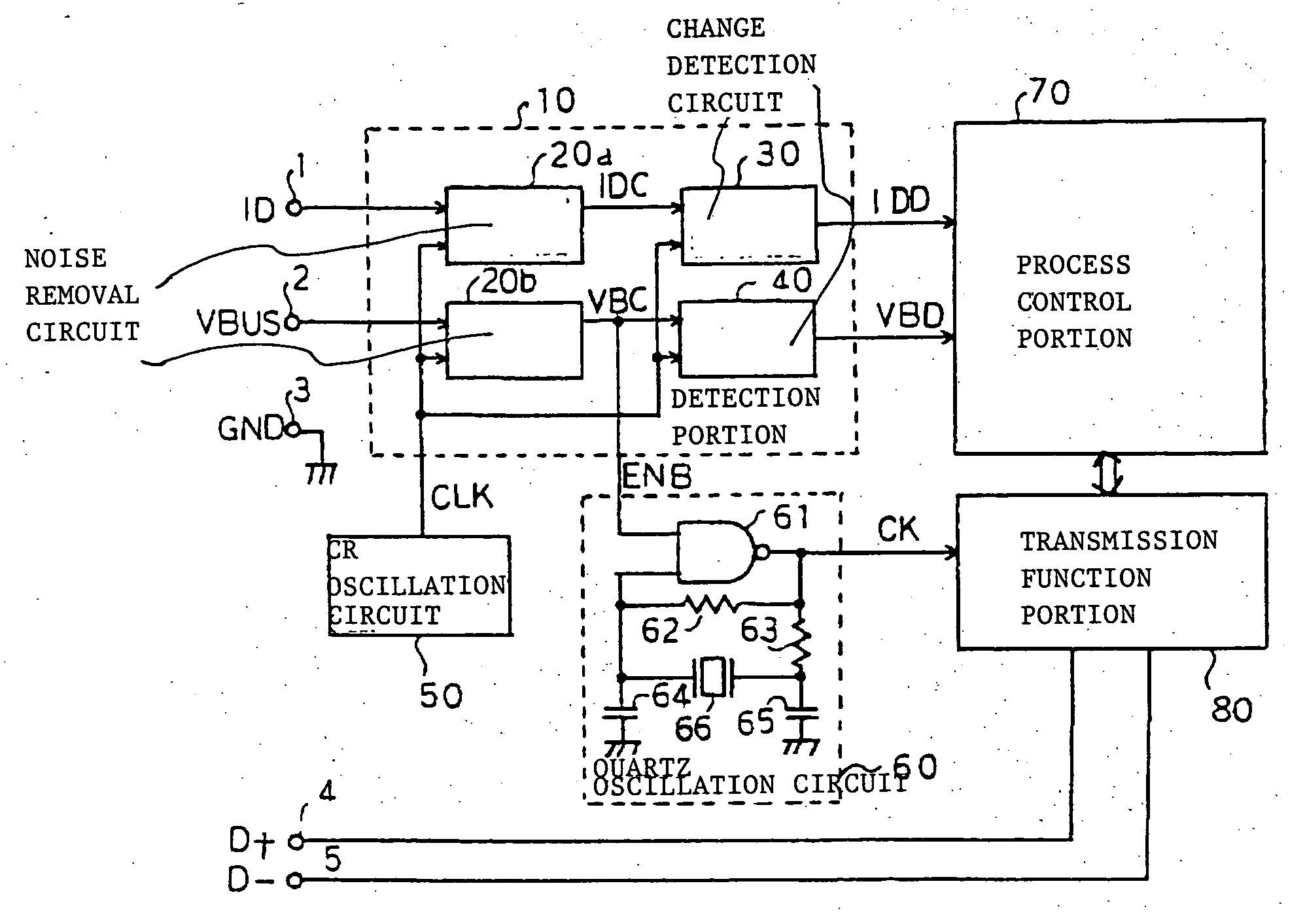
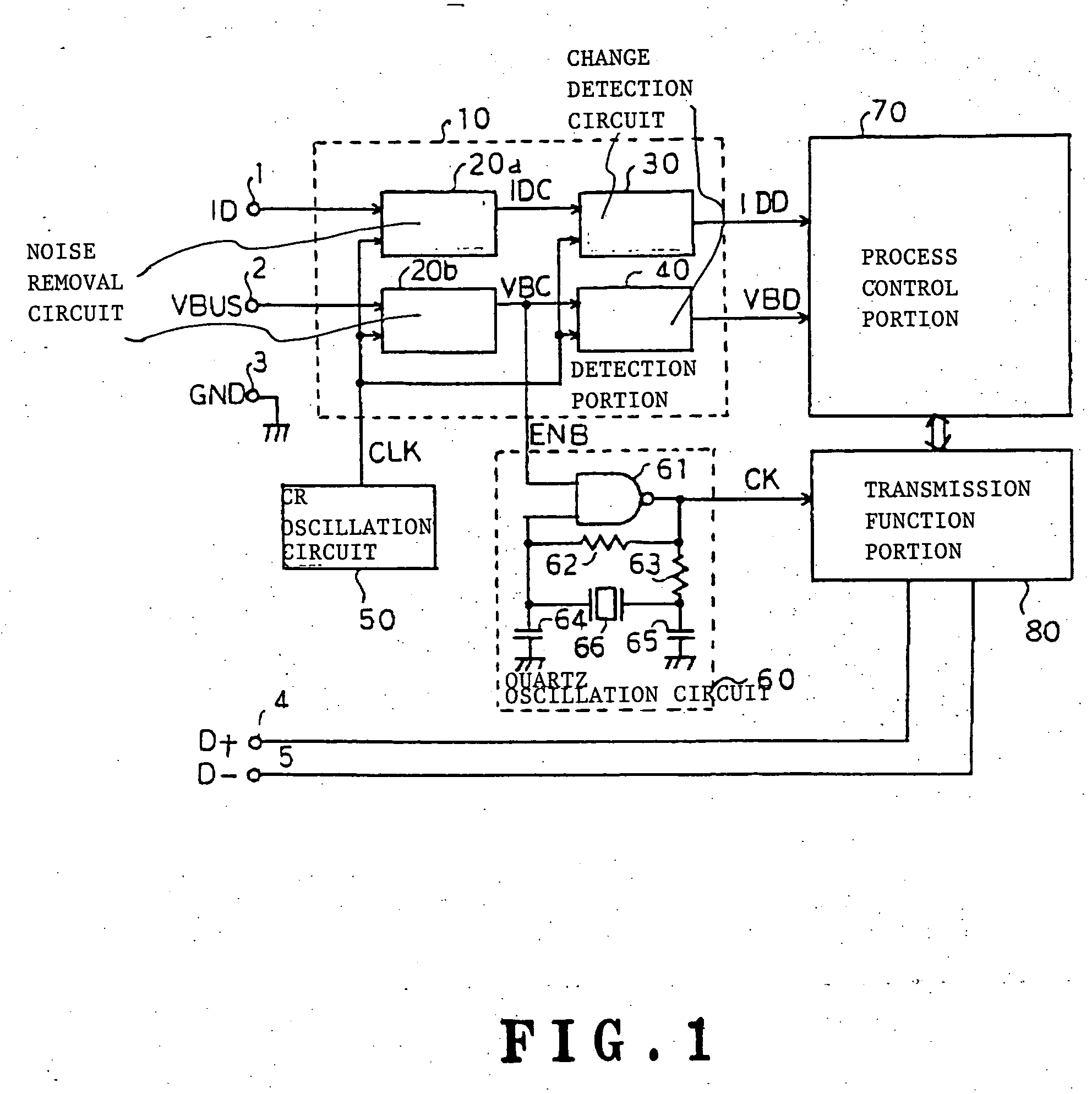
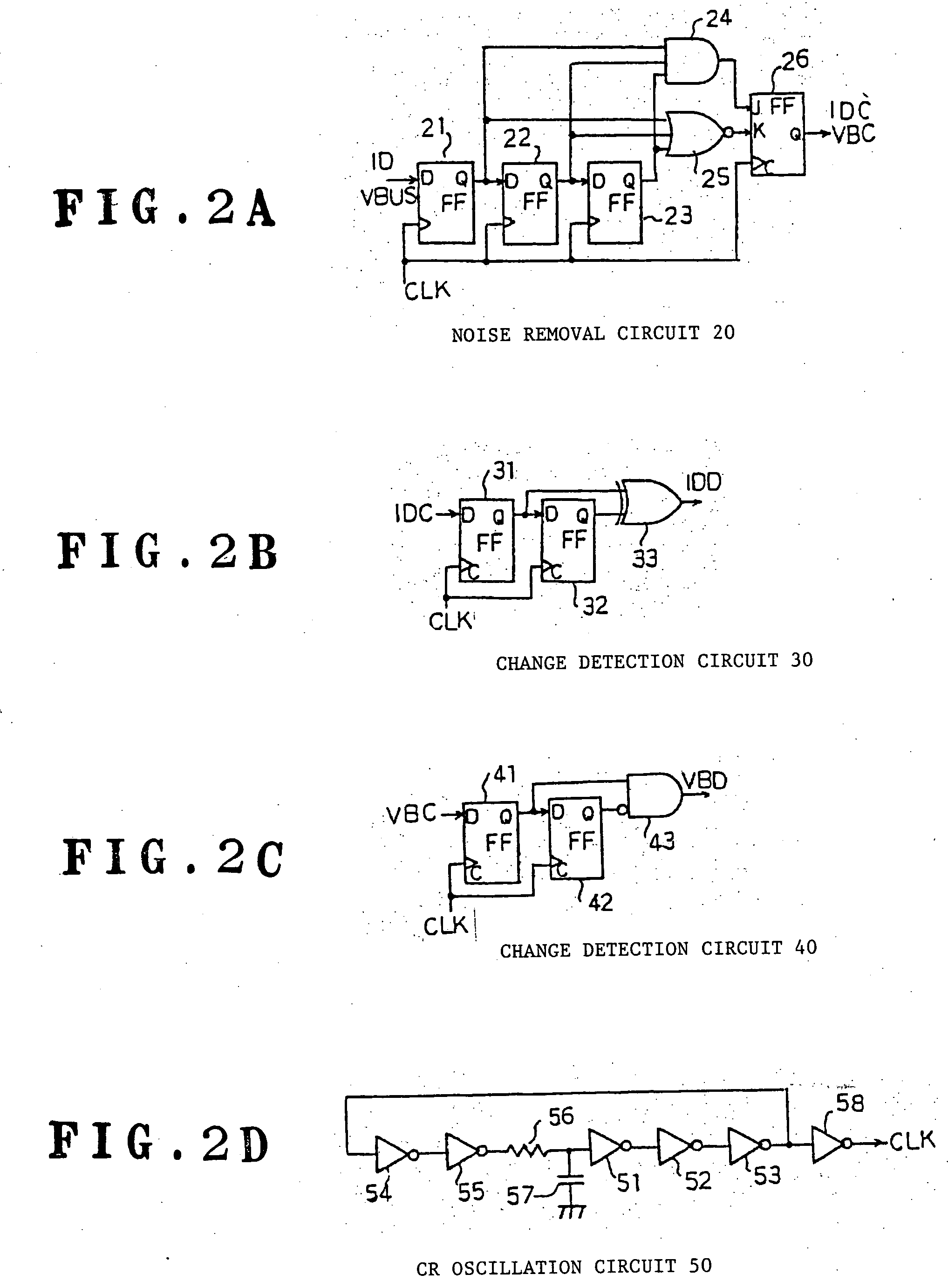
[0026] FIG. 1 is a block diagram of a USB interface circuit according to the present invention.
[0027] The USB interface circuit is OTG compliant and is provided with terminals 1 to 5 for connecting via cable one peripheral device to another. The terminal 1 receives a signal ID that designates master or slave. When the ground potential GND is provided, master is designated, and, when the ground potential GND is not received, slave is designated.
[0028] Terminal 2 sends or receives a signal VBUS that designates whether or not there is a data transmission. When there is a data transmission, an "H" signal VBUS is output from the master side, and the slave side receives the signal VBUS and is able to determine whether or not there is a data transmission. It should be noted that the pull-up circuit for the terminal 1 and the signal VBUS output circuit for the terminal 2 are omitted in this diagram.
[0029] Terminal 3 transmits a ground potential GND that is common to both the opposing periph...
second embodiment
[0053] FIG. 3 is a block diagram of a USB interface circuit according to a second embodiment of the present invention. Common reference numerals are attached to elements that are equivalent to the elements in FIG. 1.
[0054] In the USB interface circuit, the CR oscillation circuit 50 in FIG. 1 is eliminated. Additionally, edge detection circuits 90a and 90b are provided instead of the detection portion 10. Further, instead of the process control portion 70, a process control portion 70A which has a function different from the process control portion 70 is provided.
[0055] The edge detection circuits 90a and 90b respectively detect changes in the signals ID and VBUS, and the circuits have the same circuit configuration.
[0056] For example, the edge detection circuit 90a is provided with an FF 91 which has a data terminal fixed at "H" and a clock terminal to receive a signal ID. The output terminal of the FF 91 is connected to the clock terminal of an FF 92, as well as to one of the input...
third embodiment
[0068] FIG. 5 is a block diagram of a USB interface circuit according to a third embodiment of the present invention. Common reference numerals are attached to elements that are the same as in FIG. 1.
[0069] In the USB interface circuit, the CR oscillation circuit 50 in FIG. 1 is not provided. Moreover, instead of the detection portion 10 and the process control portion 70, a detection portion 10A and a process control portion 70B of different functions are provided.
[0070] The detection portion 10A is provided with an FF 11 and 12 which respectively hold expected values EX1 and EX2 supplied from the process control circuit 70B in accordance with a write signal WR received from the process control portion 70B. The output terminal of the FF 11 is connected to an EOR 13 which constitutes a comparator circuit, so that the signal ID that is input at the terminal 1 is compared with the output of the FF 11. Also, the output terminal of the FF 12 is connected to an EOR 14 which constitutes a...
PUM
 Abstract
Description
Claims
Application Information