Hillock-free gate layer and method of manufacturing the same

a gate layer and hillock-free technology, applied in the direction of semiconductor devices, electrical equipment, semiconductor/solid-state device details, etc., can solve the problems of aluminum having a lower melting point than other metals, increased process cost, and gate layer hillock generation

Inactive Publication Date: 2004-07-22
INNOLUX CORP
View PDF3 Cites 9 Cited by
  • Summary
  • Abstract
  • Description
  • Claims
  • Application Information

AI Technical Summary

Problems solved by technology

However, using expensive molybdenum or chromium will increase the cost of the process.
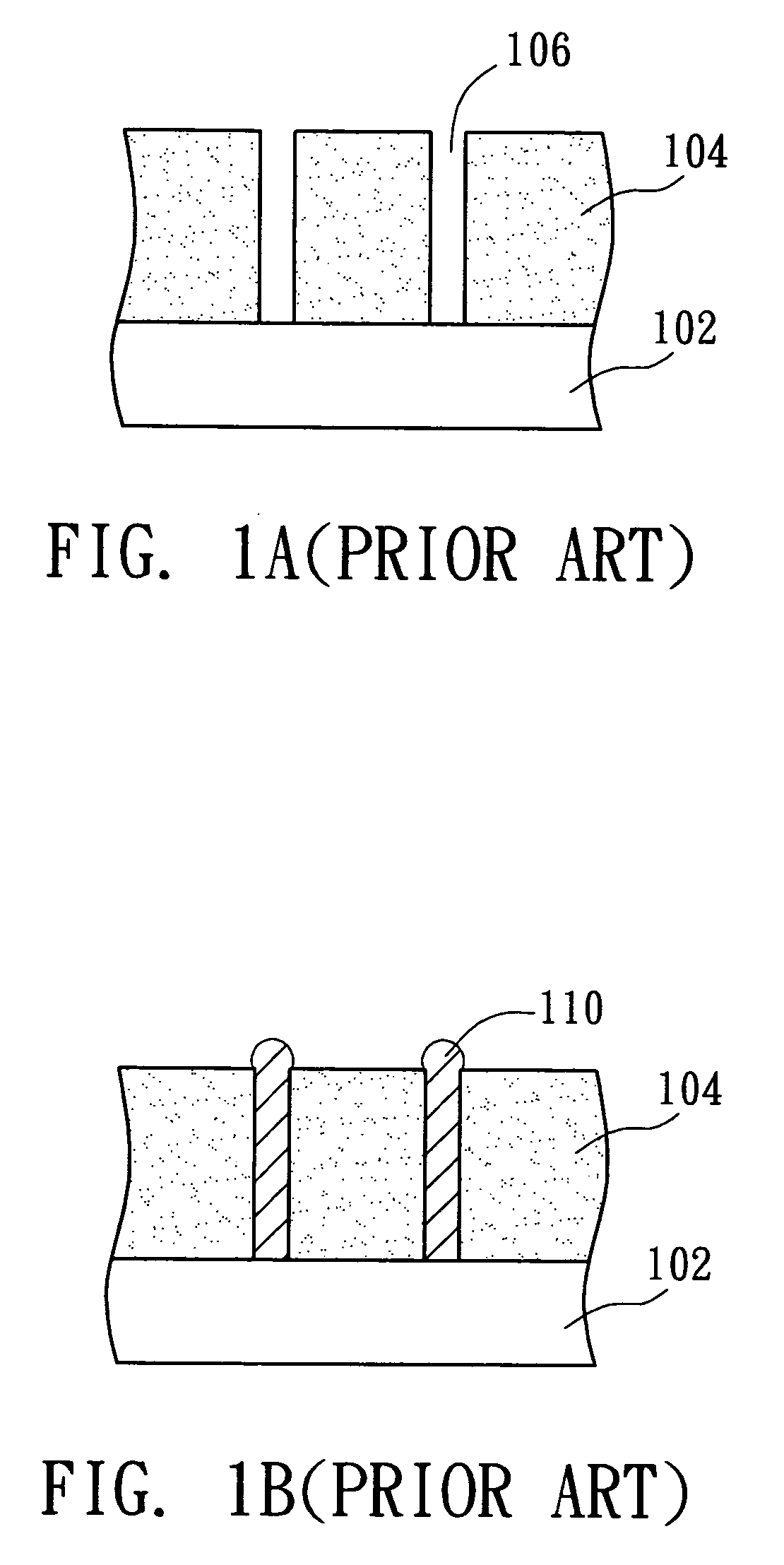
However, when aluminum is used to make the gate layer, it gives rise to an issue that hillocks are generated on the surface of the gate layer.
However, aluminum has a lower melting point than other metals, and this is a disadvantage when it is used to make a gate layer.
A problem with hillocks mentioned above occurs as aluminum is used to make the gate layer.
In practical applications, the pure aluminum layers can also include other elements, but that will be more costly than using pure aluminum layers.

Method used


Image

  • Hillock-free gate layer and method of manufacturing the same
  • Hillock-free gate layer and method of manufacturing the same
  • Hillock-free gate layer and method of manufacturing the same

Examples


experiment 2 (

[0025] Experiment 2 (for comparison):

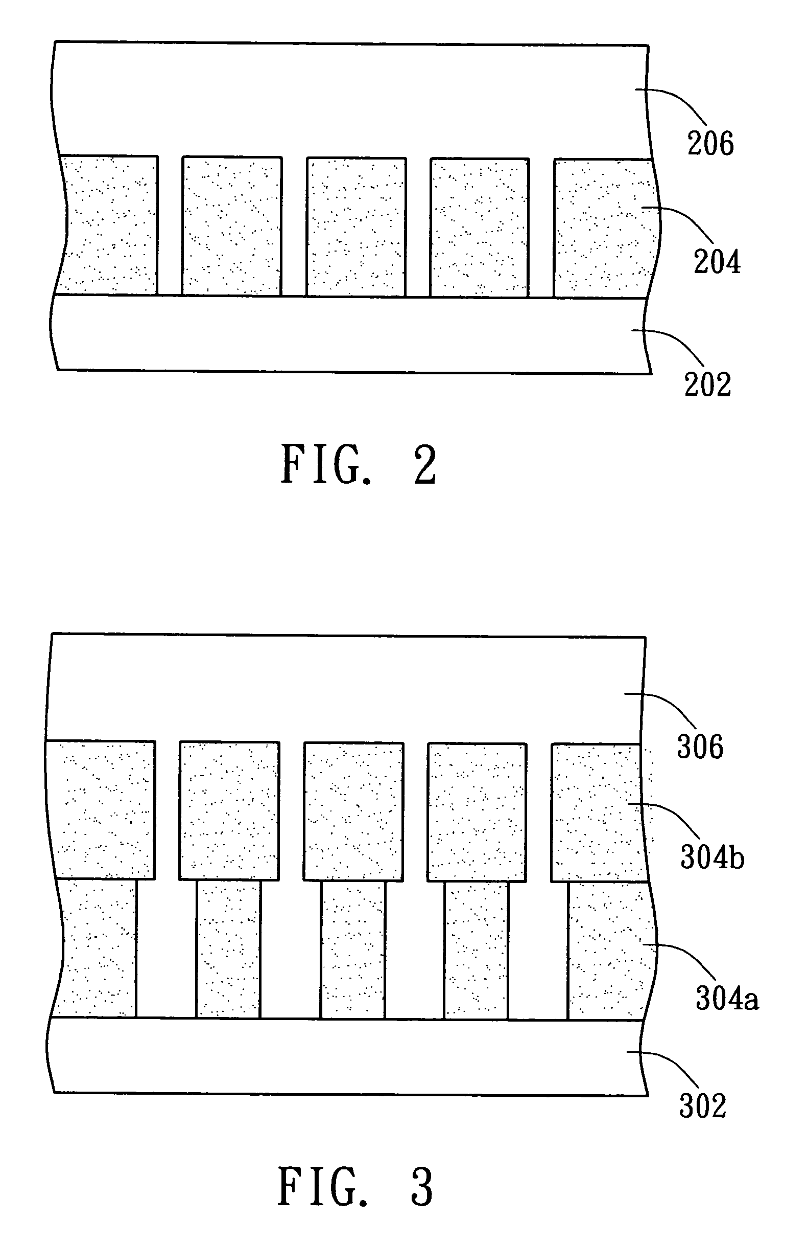
[0026] One pure aluminum layer is deposited on the substrate under the pressure 4 Pa and the sputtering power 6.5 W / cm.sup.2. An aluminum layer containing nitrogen is then formed on the pure aluminum layer. It is then annealed for one hour at a temperature of 350.degree. C.; the upper surface of the aluminum layer is observed by a scanning electron microscope to detect the presence of hillocks. The experiment results show that a few hillocks will be generated as the pressure is increased but the sputtering power is not lowered.

experiment 3

[0027]

[0028] One pure aluminum layer is deposited on the substrate under the pressure 4 Pa and the sputtering power 2.0 W / cm.sup.2. An aluminum layer with nitrogen is then formed on the pure aluminum layer. It is annealed for an hour at 350.degree. C.; the upper surface of the aluminum layer is observed with a scanning electron microscope to detect the formation of hillocks. The experiment results show that hillock surfaces will be prevented as the pressure is increased and the sputtering power is lowered.

experiment 4

[0029]

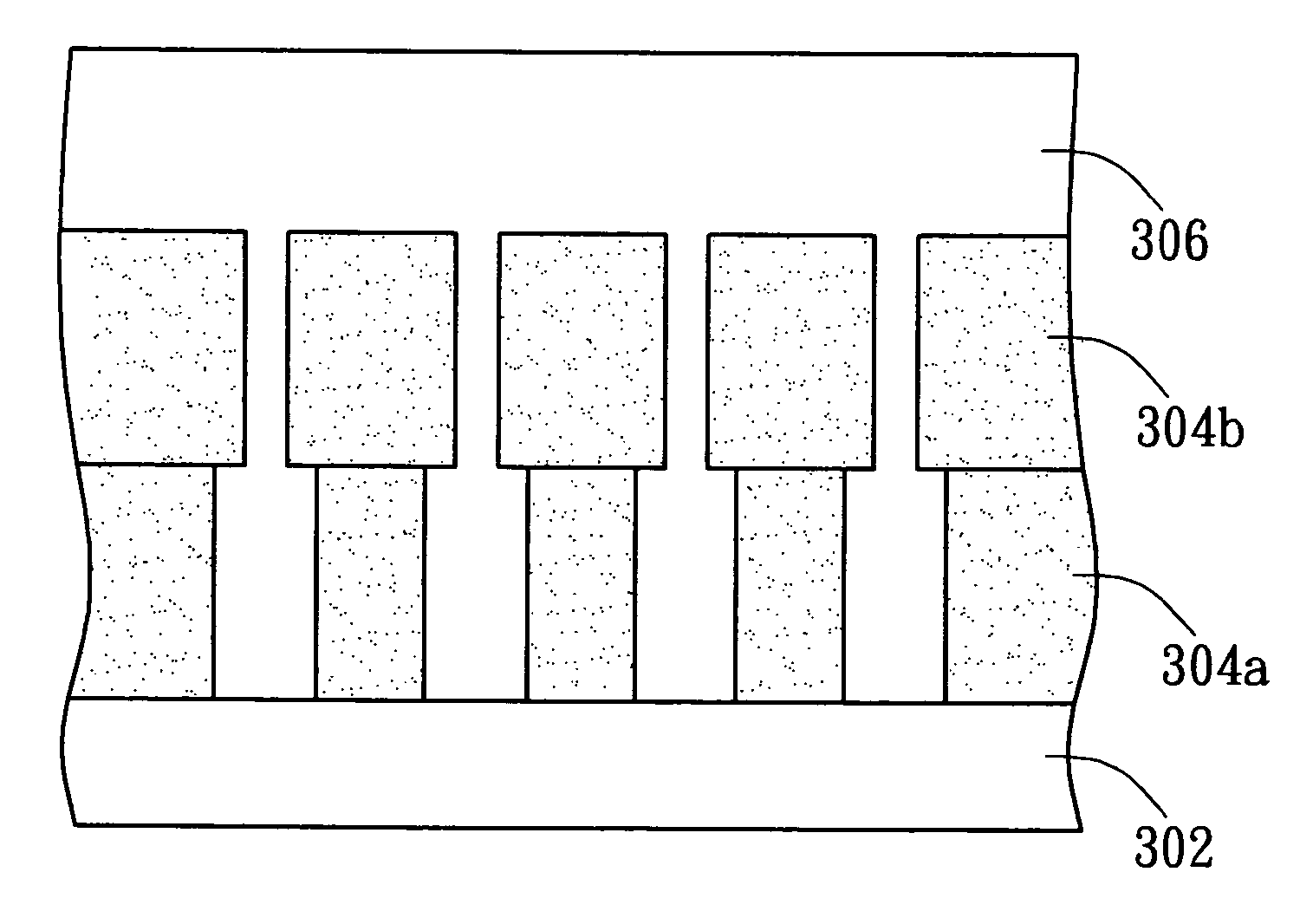
[0030] A first pure aluminum layer is deposited on the substrate under the pressure 4 Pa and the sputtering power 2.0 W / cm.sup.2. A second pure aluminum layer is, subsequently, deposited on the first pure aluminum layer under the film formation pressure 4 Pa and the sputtering power 6.5 w / cm.sup.2. An aluminum layer with nitrogen is then formed on the second pure aluminum layer. After the substrate is annealed for an hour at 350.degree. C., the upper surface of the aluminum layer is observed with a scanning electron microscope to detect the presence of hillocks. The experiment results show that as multiple pure aluminum layers are formed under high pressure and increasing sputtering power, no hillocks are generated.


PUM

PropertyMeasurementUnit
pressureaaaaaaaaaa
thicknessaaaaaaaaaa
pressureaaaaaaaaaa

Abstract

A hillock-free gate layer and method of manufacturing the same is disclosed. One or more pure aluminum layers are formed under high pressure and low sputtering power. An aluminum layer containing nitrogen is then formed on the pure aluminum layers to prevent the formation of hillocks and to reduce manufacturing costs.

Description

[0001] This application claims the benefit of Taiwan application Serial No. 92100927, filed Jan. 16, 2003.[0002] 1. Field of the Invention[0003] The invention relates in general to a conducting layer of aluminum, and more particularly to a hillock-free gate layer and method of manufacturing the same.[0004] 2. Description of the Related Art[0005] In semiconductor manufacturing process, either molybdenum (Mo) or chromium (Cr) is usually selected to make a gate layer. However, using expensive molybdenum or chromium will increase the cost of the process. Aluminum, the most plentiful mineral metal on earth, is cheap, easily accessible, and is usually used to make metal layers. However, when aluminum is used to make the gate layer, it gives rise to an issue that hillocks are generated on the surface of the gate layer.[0006] The advantages of aluminum when it is used in semiconductor manufacturing process are that aluminum has a low resistance, good adhesion to the substrate, and better et...

Claims


Application Information

Patent Timeline
Patent Type & Authority Applications(United States)
IPC IPC(8): H01L21/28H01L21/3205H01L23/532H01L29/423
CPCH01L21/28H01L29/42316H01L23/53223H01L21/32051H01L2924/0002H01L2924/00
Inventor WANG, CHENG-CHI
Owner INNOLUX CORP
Why Eureka
Try Eureka