

Technique for suppression of latchup in integrated circuits (ICS)
a technology of integrated circuits and latchups, which is applied in the direction of electrical apparatus, semiconductor devices, semiconductor/solid-state device details, etc., can solve the problems of permanent damage to the target affecting the electrical properties of silicon, etc., and achieves the reduction or elimination of the sensitivity of the latchup of the integrated circuit on this wafer or die, and the cost impact of the procedure on commercial production. , the effect of avoiding the cost impa
- Summary
- Abstract
- Description
- Claims
- Application Information
AI Technical Summary
Benefits of technology
Problems solved by technology
Method used
Image

Examples
Embodiment Construction
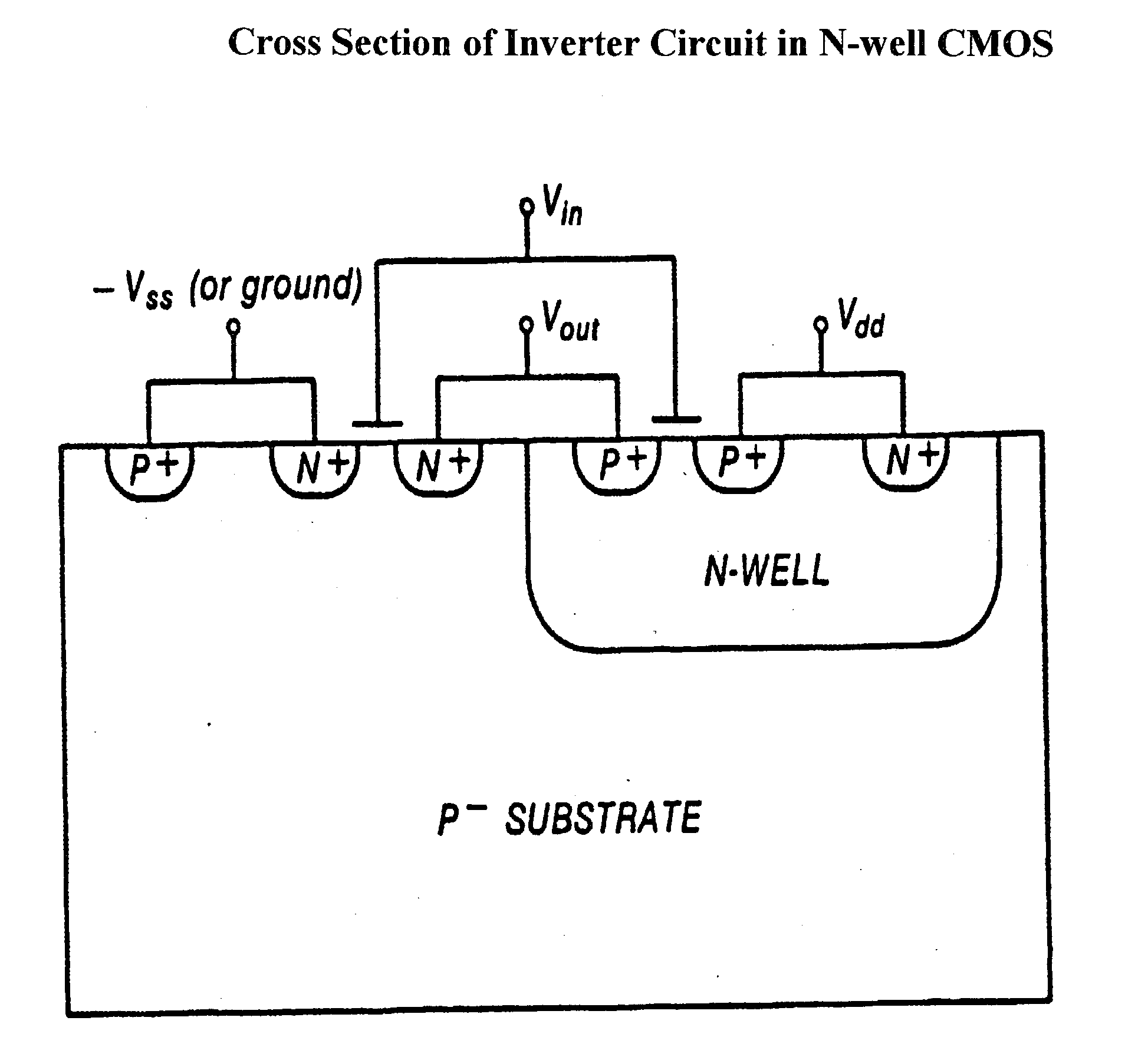
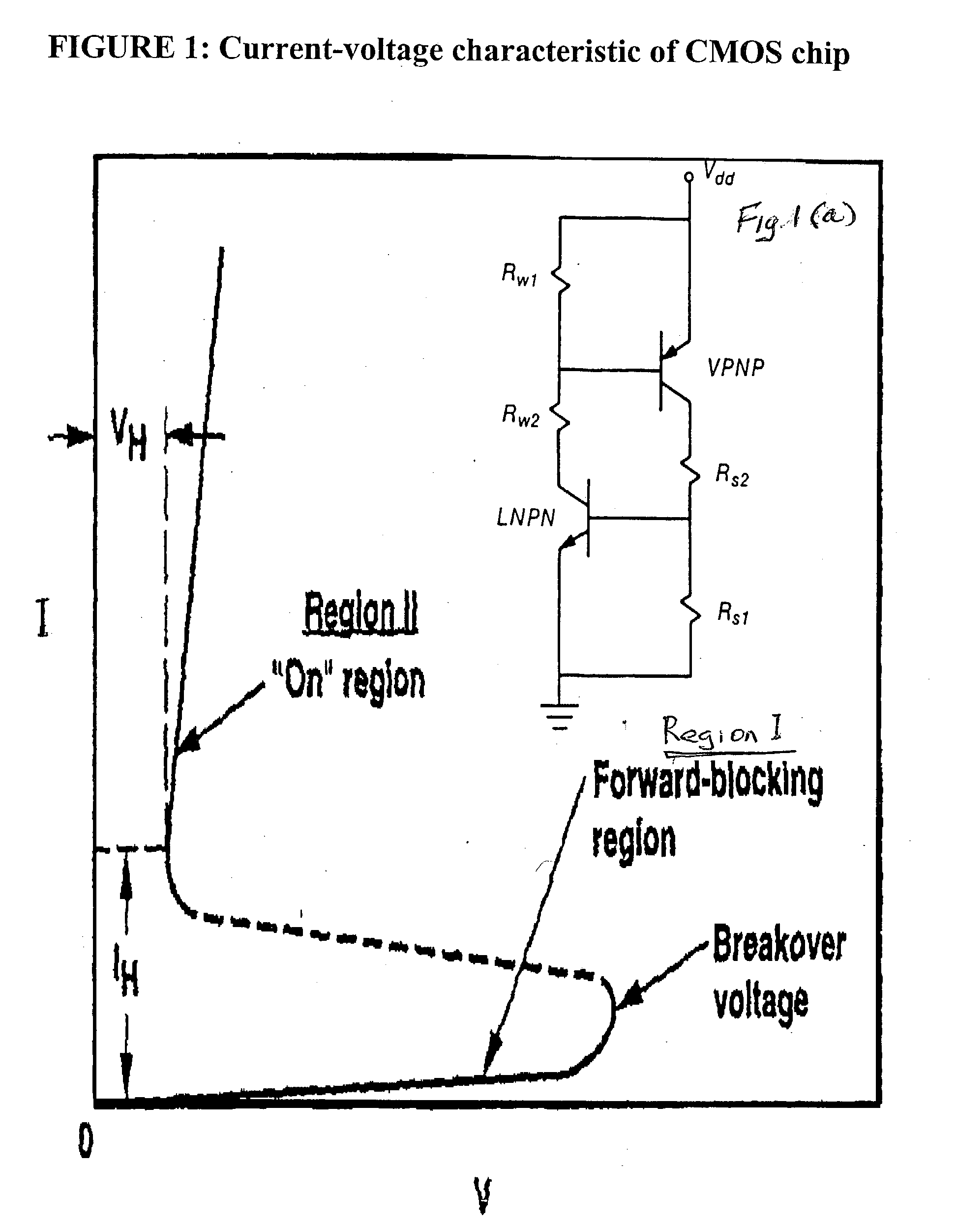
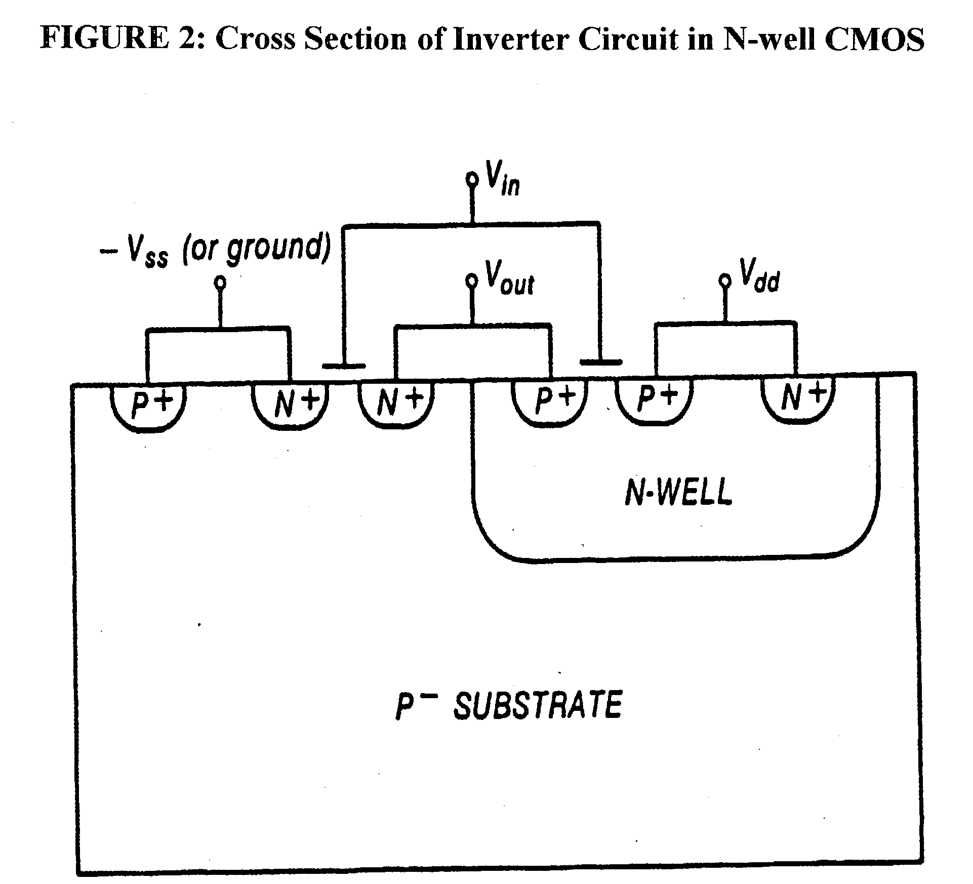
[0061] According to the present invention, there are three approaches, utilizing ion implantation through the back surface of an integrated circuit, that can be pursued to suppress latchup. The first reduces current flow due to photocurrent across the well junction. Degrading the minority carrier lifetime near the well junction will reduce the photo-current, and thus reduce the likelihood that latchup will occur. The second approach reduces the voltage drop that a given amount of current across the well junction will produce in the junctions of the parasitic bipolar devices by increasing the conductivity of the silicon. This is done by implanting ions which are electrically conducting near the well junction. The third approach degrades the common base current gain of one or more of the parasitic bipolar transistors so that the loop gain of the PNPN configuration can not exceed unity. This is done by exploiting the crystalline damage that results from ion implantation. The current ga...
PUM
 Abstract
Description
Claims
Application Information