Method for fluorocarbon film depositing

a fluorocarbon film and depositing technology, applied in the direction of chemical vapor deposition coating, semiconductor/solid-state device details, coatings, etc., can solve the problems of reducing interconnect separation and geometries, undetected augmentation of capacitance (c) and resistance (r), respectively, of interconnect structures, and cross-talk nois

Inactive Publication Date: 2004-08-19
MACRONIX INT CO LTD
View PDF2 Cites 15 Cited by
  • Summary
  • Abstract
  • Description
  • Claims
  • Application Information

AI Technical Summary

Problems solved by technology

Reduced interconnect separations and geometries, however, can undesirably augment capacitances (C) and resistances (R), respectively, of the interconnect structures.
These increased electrical properties can introduce, for example, cross talk noise and propagation delays between interlevel and intralevel conductive interconnects.
However, plasma enhanced CVD processes can be relatively difficult to control.
In particular, the formation of a suitably thin and / or optimally distributed layer of fluorocarbon onto a semiconductor substrate, with for example a relatively low dielectric value, can be difficult.
For instance, conventional depositions of a fluorocarbon film onto a substrate can entail multiple processes and can result in relatively poor control of the thickness of the deposited film over different portions of the substrate.
When the substrate comprises features, such as photoresist features or other patterned blocks, the relatively poor control can be particularly prevalent.
In addition, conventional plasma enhanced CVD reactors may require relatively high temperatures for the deposition of a fluorocarbon film onto the surface of a substrate.
In cases where the substrate comprises organic materials, such as substrates having photoresist features, the high temperatures may undesirably damage the organic material.

Method used


Image

  • Method for fluorocarbon film depositing
  • Method for fluorocarbon film depositing
  • Method for fluorocarbon film depositing

Examples


Embodiment Construction

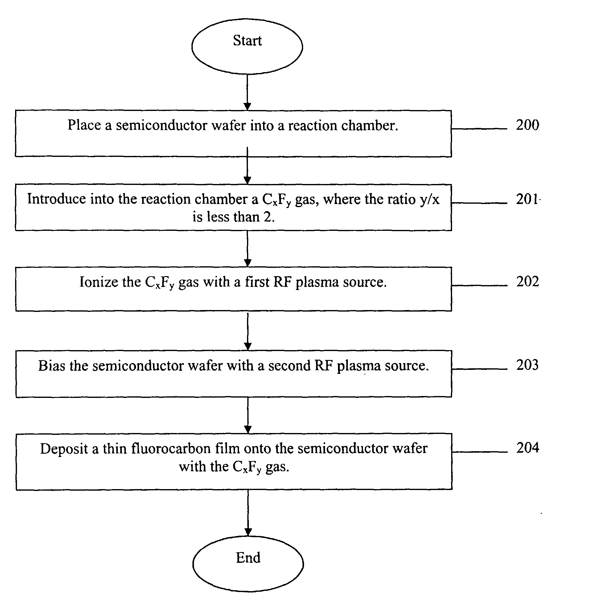
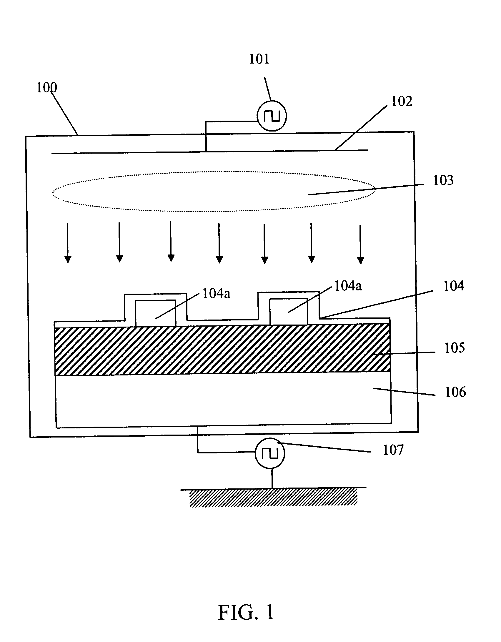
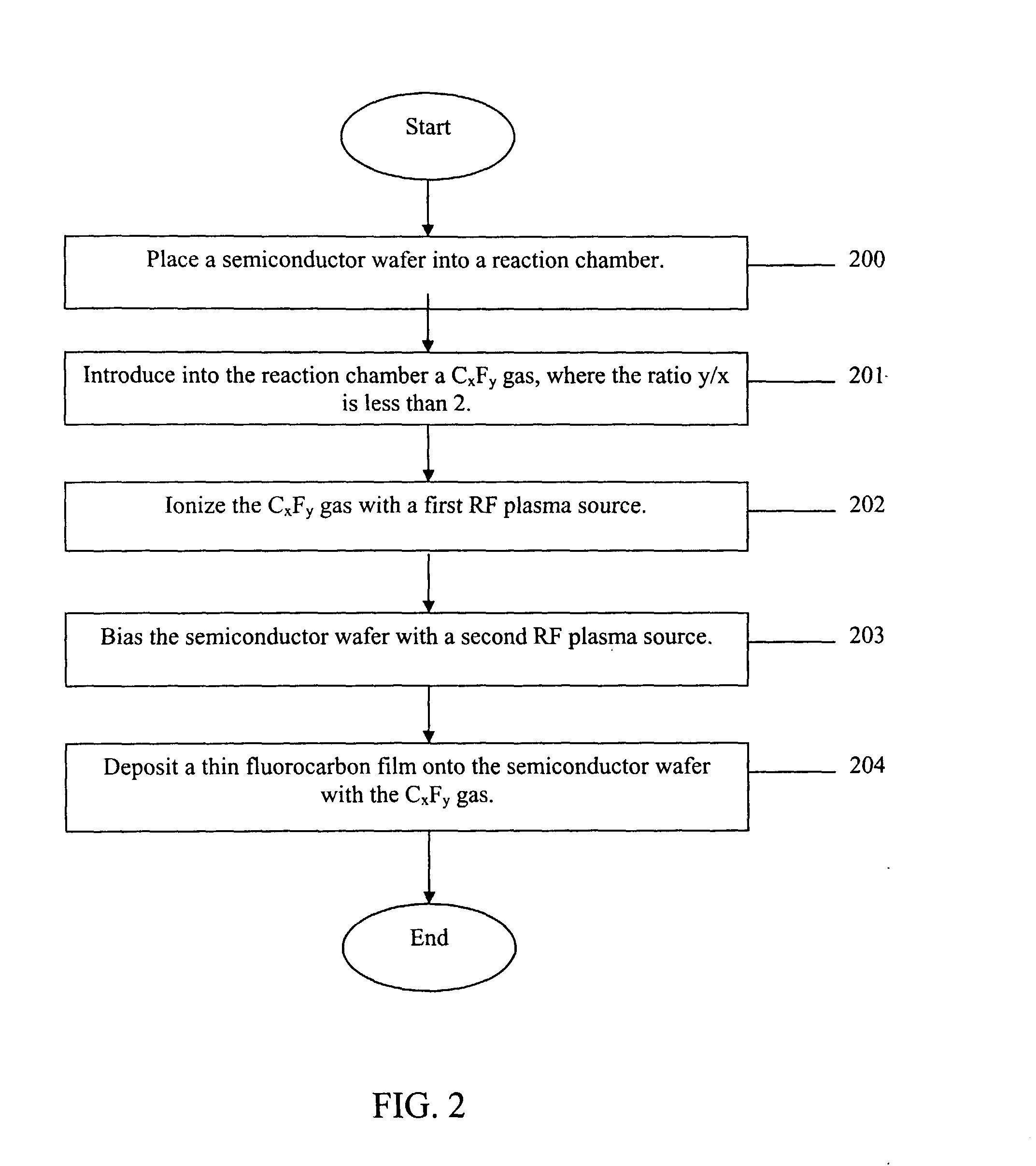
[0024] Reference will now be made in detail to the presently preferred embodiments of the invention, examples of which are illustrated in the accompanying drawings. Wherever possible, the same reference numbers are used in the drawings and the description to refer to the same or like parts. It should be noted that the drawings are in greatly simplified form and are not to precise scale. In the following description, numerous specific details are set forth illustrating Applicants' best mode for practicing the invention and enabling one of ordinary skill in the art to make and use the invention. It will be understood, however, to one skilled in the art that the present invention may be practiced in certain applications without these specific details. Thus, the illustrated embodiments set forth herein are presented by way of example and not by way of limitation

[0025] The intent of the following detailed description is to cover all modifications, alternatives, and equivalents as may fal...


PUM

PropertyMeasurementUnit
frequencyaaaaaaaaaa
poweraaaaaaaaaa
frequenciesaaaaaaaaaa

Abstract

A thin fluorocarbon layer is deposited onto the surface of a substrate through the application of a plasma enhanced chemical vapor deposition process, wherein the substrate is placed on a chuck within a reaction chamber and fluorocarbon gas is introduced into the reaction chamber under the influence of a first plasma source and a second plasma source. The fluorocarbon gas is a CxFy gas, wherein the ratio y/x is less than 2. The plasma source ionizes the fluorocarbon gas by applying RF plasma energy, and the second plasma source applies a self-bias to the substrate at an RF frequency. The ionized fluorocarbon is deposited onto and adheres to the substrate to form a thin film of fluorocarbon on the substrate.

Description

[0001] 1. Field of the Invention[0002] The present invention relates generally to insulating structures for use on semiconductor substrates and, more particularly, to plasma enhanced chemical vapor deposition methods for forming thin dielectric layers on integrated circuits.[0003] 2. Description of Related Art[0004] As integrated circuit devices are progressively miniaturized and packaged closer together, the number and density of interconnects commensurately increases. Smaller interline and interlevel separations of these interconnects (e.g., conductive lines and vias), coupled with reduced interconnect geometries, help to facilitate the greater interconnect densities.[0005] Reduced interconnect separations and geometries, however, can undesirably augment capacitances (C) and resistances (R), respectively, of the interconnect structures. These increased electrical properties can introduce, for example, cross talk noise and propagation delays between interlevel and intralevel conduc...

Claims


Application Information

Patent Timeline
Patent Type & Authority Applications(United States)
IPC IPC(8): C23C16/30H01L21/31H01L21/312H01L21/314H01L21/768H01L23/522
CPCC23C16/30H01L21/3127H01L21/02274H01L21/0212
Inventor TSAI, HSIN-YILIANG, MING CHUNG
Owner MACRONIX INT CO LTD
Why Eureka
Try Eureka