
Buffer circuit and active matrix display using the same

a buffer circuit and active matrix technology, applied in logic circuit coupling/interface arrangement, pulse technique, instruments, etc., can solve the problems of increasing power consumption and increasing power consumption, and achieve the effect of reducing power consumption

Active Publication Date: 2004-08-26
SAMSUNG DISPLAY CO LTD
View PDF8 Cites 33 Cited by
  • Summary
  • Abstract
  • Description
  • Claims
  • Application Information

AI Technical Summary

Benefits of technology

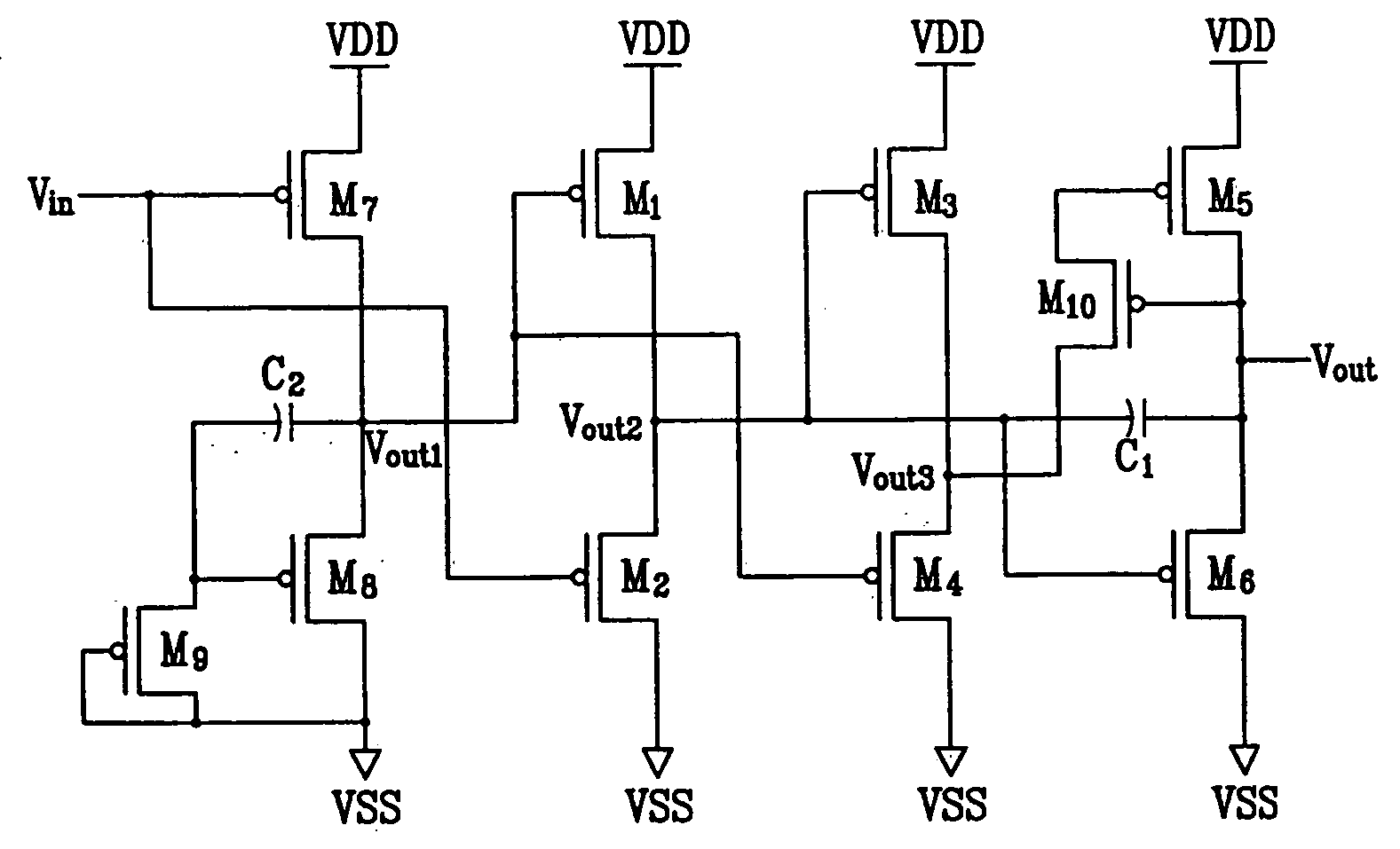
The present invention provides a buffer circuit with reduced power consumption and desired voltage levels. This is achieved by employing bootstrapping, which involves a transistor circuit that uses a second voltage level to generate the first voltage level. The buffer circuit includes a first transistor, a second transistor, a third transistor, a fourth transistor, and a fifth transistor. A capacitance is formed between the output end and the second power source. The buffer circuit can be used in an active matrix display to drive the display panel. The technical effects of the invention include reduced power consumption, desired voltage levels, and improved display quality.

Problems solved by technology

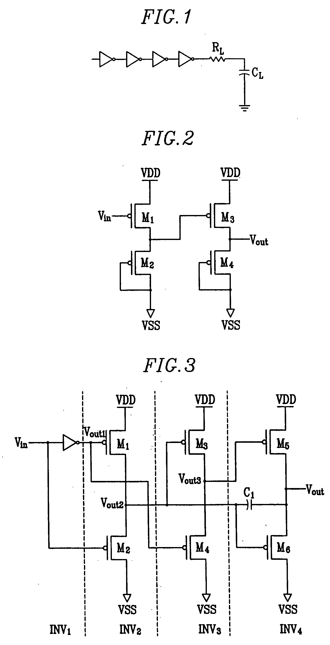
Since the transistors M3 and M4 are concurrently turned on, a static current flows through the transistors M3 and M4, thereby increasing power consumption.
As a result, the power consumption increases due to the static current flowing through inverters which is great for the second stage according to characteristics of the buffer circuit.

Method used


Image

  • Buffer circuit and active matrix display using the same
  • Buffer circuit and active matrix display using the same
  • Buffer circuit and active matrix display using the same

Examples


Embodiment Construction

[0036] In the following detailed description, only certain exemplary embodiments of the present invention are shown and described, by way of illustration. As those skilled in the art would recognize, the described exemplary embodiments may be modified in various different ways, all without departing from the spirit or scope of the present invention. Accordingly, the drawings and description are to be regarded as illustrative in nature, and not restrictive.

[0037] Exemplary embodiments of a buffer circuit and a flat panel display using the same will be described in detail in reference to the drawings.

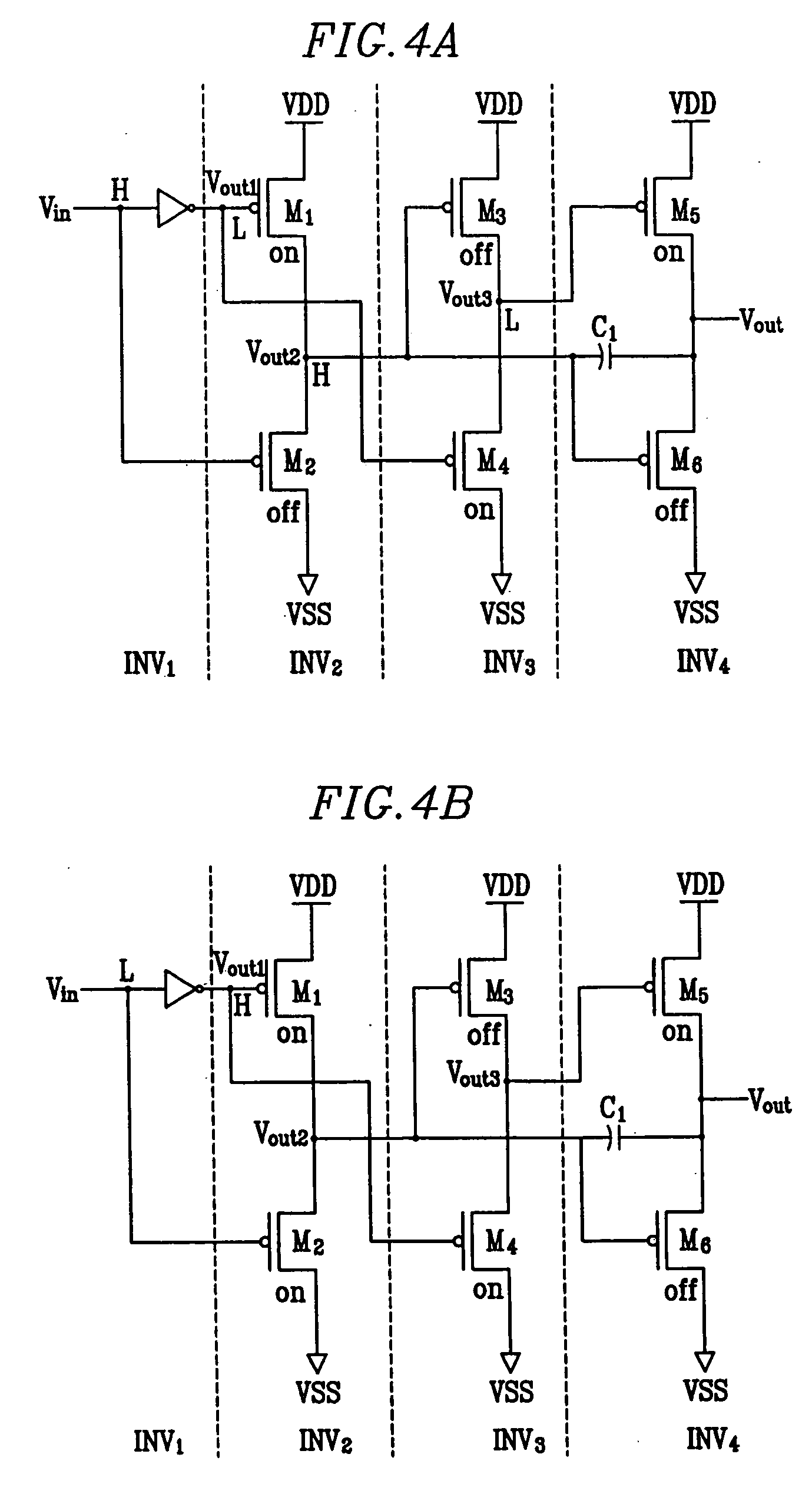
[0038] Referring to FIGS. 3 through 4D, a buffer circuit in one exemplary embodiment of the present invention will be described. FIG. 3 shows a circuit diagram of a buffer circuit according to an exemplary embodiment of the present invention, and FIGS. 4A through 4D show an operation of the buffer circuit according to the exemplary buffer circuit of FIG. 3.

[0039] As shown in FIG. 3, the b...


PUM


Abstract

A buffer circuit includes first to sixth transistors. The first transistor is coupled between a first power source and a first node, and has a gate for receiving a first signal having a first signal level. The second transistor is coupled between the first node and a second power source, and has a gate for receiving a second signal having a second signal level, which is an inverse of the first signal level. The third transistor has a gate coupled to the first node, and is coupled between the first power source and a second node. The fourth transistor is coupled between the second node and the second power source, and has a gate for receiving the first signal. The fifth transistor has a gate coupled to the second node, and is coupled between the first power source and an output end. The sixth transistor has a gate coupled to the first node, and is coupled between the output end and the second power source. In addition, a capacitance is formed between the gate of the sixth transistor and the output end.

Description

CROSS REFERENCE TO RELATED APPLICATION[0001] This application claims priority to and the benefit of Korean Patent Application No. 2003-11418 filed on Feb. 24, 2003 in the Korean Intellectual Property Office, the content of which is incorporated herein by reference.BACKGROUND OF THE INVENTION[0002] (a) Field of the Invention[0003] The present invention relates to a buffer circuit and an active matrix display using the same.[0004] (b) Description of the Related Art[0005] Active matrix displays, image sensors, and semiconductor memories use a shift register circuit and a buffer circuit to supply scan signals. When the shift register circuit has a large load or capacitance, a buffer circuit is installed between the shift register circuit and the load. The usage of the buffer circuit increases the magnitude of the current for charging and discharging the load, thereby increasing operation rates. If the buffer circuit becomes larger according to the load size, the capacitance at an input ...

Claims


Application Information

Patent Timeline
Patent Type & Authority Applications(United States)
IPC IPC(8): H03K17/16G09G3/20G11C19/00G11C19/18G11C19/28H03F1/56H03K17/00H03K17/687H03K19/00H03K19/017H03K19/0175H03K19/0185H03K19/0944
CPCG09G3/20G09G2310/0267G09G2310/0289G09G2330/021H03K19/018521G11C19/184G11C19/28H03K19/0013H03K19/01714G11C19/00
Inventor SHIN, DONG-YONGCHUNG, BO-YONG
Owner SAMSUNG DISPLAY CO LTD
Learn More