Eureka AIR delivers breakthrough ideas for toughest innovation challenges, trusted by R&D personnel around the world.

Double buffered flash programming

Active Publication Date: 2004-09-02
MICROCHIP TECH INC
View PDF9 Cites 12 Cited by
  • Summary
  • Abstract
  • Description
  • Claims
  • Application Information

AI Technical Summary

Problems solved by technology

However, read / writes to a flash memory device may require relatively long periods of time to use in programming chips.
Because conventional flash memory devices may not be read while data is being written to the flash memory device, a flash memory device may be relatively slow for use in programming chips or even in using a computer system in normal operating mode.
Switching back and forth between programming mode can be very time consuming and therefore programming a flash memory device may be inefficient.

Method used


Image

  • Double buffered flash programming
  • Double buffered flash programming
  • Double buffered flash programming

Examples


Embodiment Construction

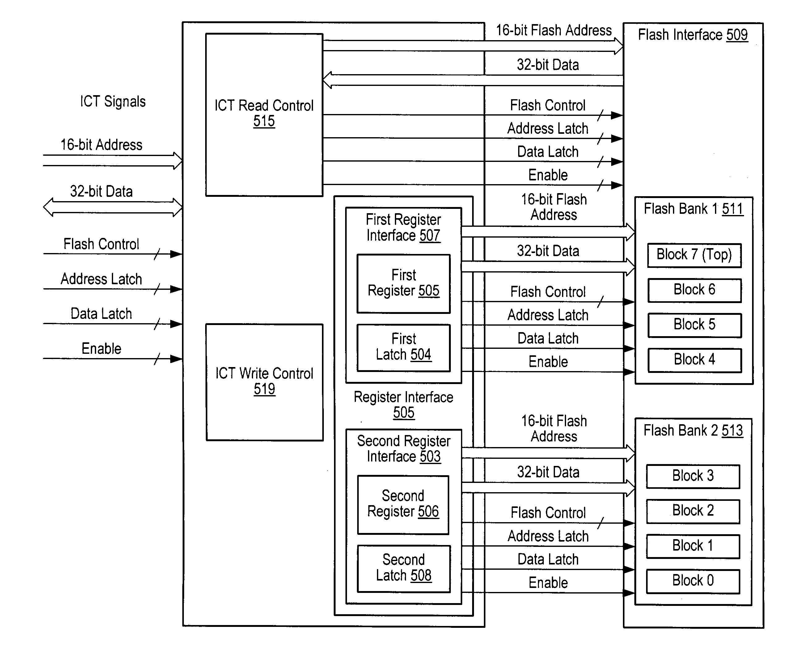
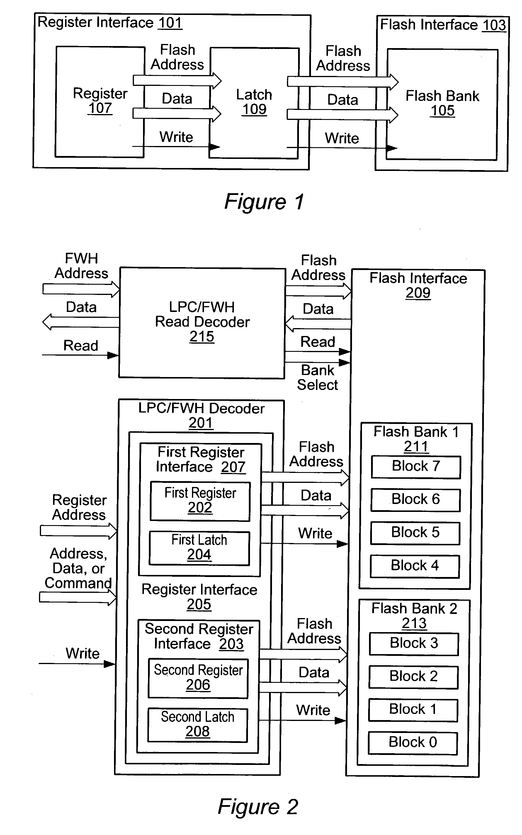
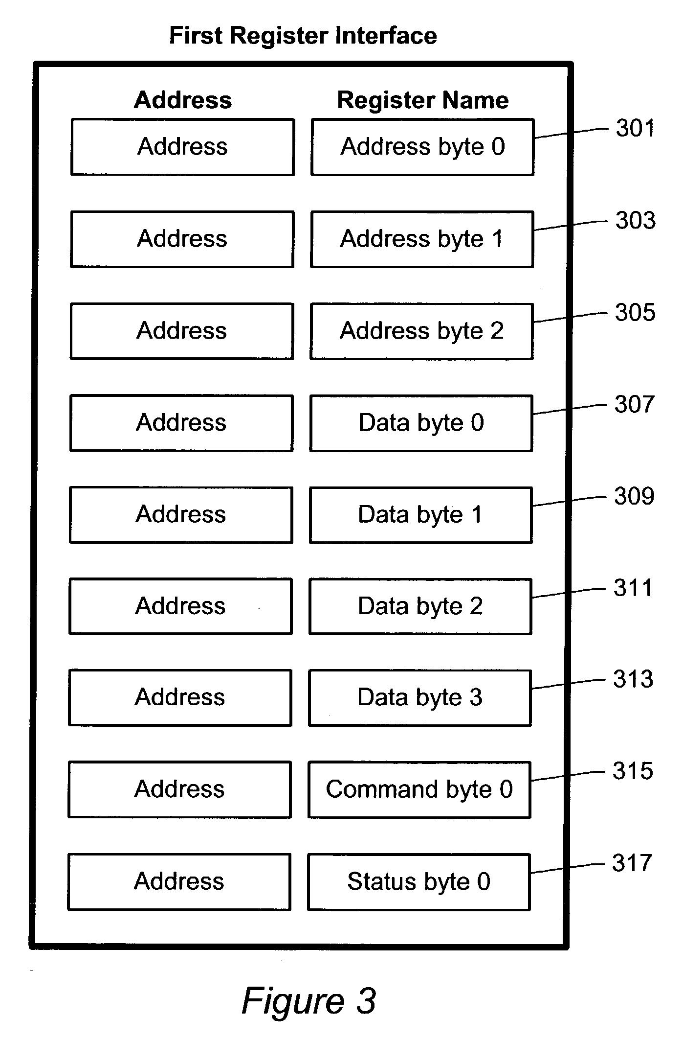
[0017] FIG. 1: Register Interface Coupled to a Flash Bank

[0018] FIG. 1 illustrates an embodiment of a register interface coupled to a flash bank. In one embodiment, a register interface 101 may be coupled to a flash bank 105 in a flash interface 103. While FIG. 1 shows one flash bank 105 in the flash interface 103, a greater number of flash banks in the flash interface 103 are also contemplated. In one embodiment, the register interface 101 may have a register 107 and a latch 109. As used herein, the term "latch" may refer to any device for latching a register 107. In one embodiment, a "latch" may refer to a flip-flop or group of flip-flops. Other latches 109 are also contemplated.

[0019] In one embodiment, the flash bank 105 may be a 2 megabit flash (256 kilobytes) partitioned into 16 kilobyte by 32 bit sections (i.e., 64 kilobyte blocks). Other sizes and partitions are also contemplated. In one embodiment, the flash bank 105 may have a page size of 2048 bytes divided in 8 rows in w...


PUM


Abstract

A double buffered flash bank. In one embodiment, a flash interface may be programmed by a register interface with a first set of data while a second set of data is being written to the register interface. In one embodiment, flash banks may be programmed in parallel using latched register interfaces. For example, while data from a first register interface is being written to the first flash bank and data from a second register interface is being written to a second flash bank, new data may be written to the first register interface and to the second register interface. The new data may then be written from the first register interface to the first flash bank and from the second register interface to the second flash bank.

Description

[0001] 1. Field of the Invention[0002] The present invention relates generally to computer system memory and specifically to flash interface in computer systems.[0003] 2. Description of the Related Art[0004] Computer systems may use flash memory devices for storing data in a non-volatile memory medium. For example, the flash memory device may be electrically erasable programmable read-only memory (EEPROM) that uses transistors to store data without requiring power to maintain the data storage. Flash memory devices may be faster than other non-volatile memories, and therefore may be used in a firmware hub (FWH) for information storage. Flash memory devices may also be used as portable memory devices and in devices requiring quick, reliable access to data such as a basic input output system (BIOS), a memory card for a digital camera, and a memory device for a video game.[0005] Flash memory devices may also be used when assembling computer systems to store programs on a motherboard. Pr...

Claims


Application Information

Patent Timeline
IPC IPC(8): G06F12/00G06F12/02G06F12/06
CPCG06F12/0607G06F12/0246
Inventor SCHOEPFLIN, ROBERT W.WAHLER, RICHARD E.STREIBER, RONALD W.VIRZI, JOHN D.NOVIELLO, DONALD D.
Owner MICROCHIP TECH INC
Why Eureka
Eureka Blog
Learn More