Light emitting device

a technology of light-emitting devices and phosphor materials, which is applied in the direction of gas-filled discharge tubes, discharge tubes/lamp details, solid cathodes, etc., can solve the problems of insufficient prevention of phosphor material degradation due to moisture, increased manufacturing costs, and increased manufacturing costs

Inactive Publication Date: 2004-10-21
TOYODA GOSEI CO LTD +1
View PDF7 Cites 122 Cited by
  • Summary
  • Abstract
  • Description
  • Claims
  • Application Information

AI Technical Summary

Benefits of technology

0017] FIG. 1 is a side view showing the conventional light emitting device;

Problems solved by technology

However, in the light emitting device as shown in FIG. 1, since the phosphor layer 3 is exposed, the phosphor material may be subjected to degradation due to absorbed moisture.
If an air-tight housing is employed to prevent the penetration of water into the cover 2, the manufacturing cost will rise since the light emitting device becomes difficult to assemble.
Even in case of dispersing phosphor particles in the sealing resin material as in Japanese patent application laid-open No. 2001-217466, the degradation of phosphor material due to moisture cannot be prevented sufficiently.
Therefore, it is difficult to make the thickness of phosphor layer 3 equal.
Thus, it is difficult to generate equal fluorescence over the entire cover 2.

Method used


Image

  • Light emitting device
  • Light emitting device
  • Light emitting device

Examples


first embodiment

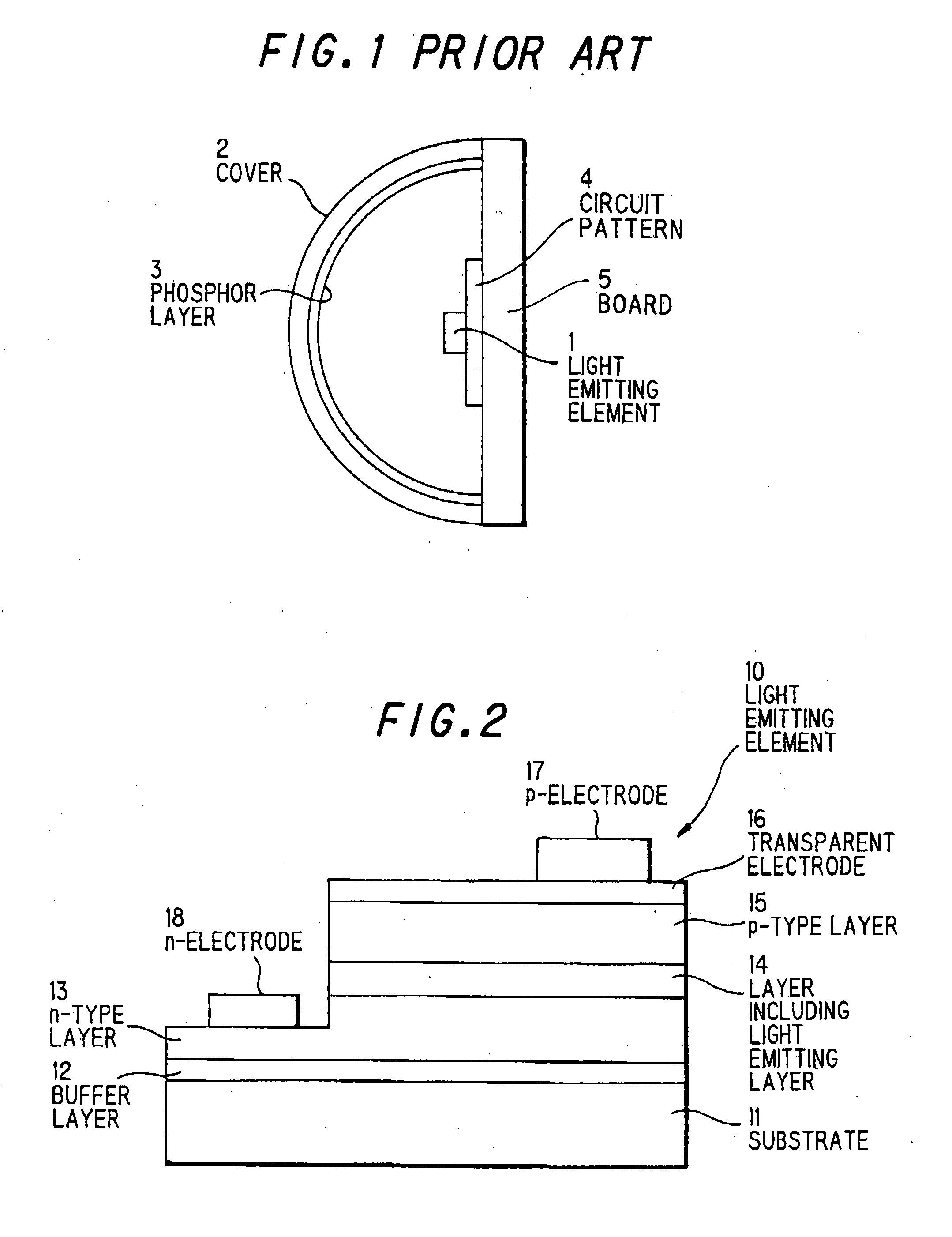
[0054] FIG. 2 is a cross sectional view showing a light emitting element 10 used in the preferred embodiments of the invention.

[0055] In this embodiment, a face-up type III group nitride system compound semiconductor light emitting element 10 as shown in FIG. 2 is used. The light emitting element 10 emits ultraviolet light. The details of layers to compose the light emitting element 10 are as follows:

1 Layers Composition p-type layer 15 p-GaN:Mg layer 14 including InGaN layer included light emitting layer n-type layer 13 n-GaN:Si buffer layer 12 AlN substrate 11 sapphire

[0056] The emission wavelength of light emitting element 10 can be adjusted by controlling the composition ratio of III group element in layer 14 including light emitting layer. Alternatively, a flip-chip type light emitting element may be used that a thick p-electrode to cover the surface of p-type layer 15 is provided instead of a transparent electrode 16 and p-electrode 17.

[0057] n-type layer 13 of GaN with n-type...

second embodiment

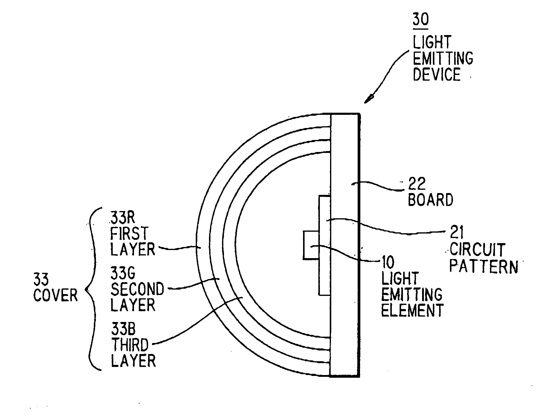
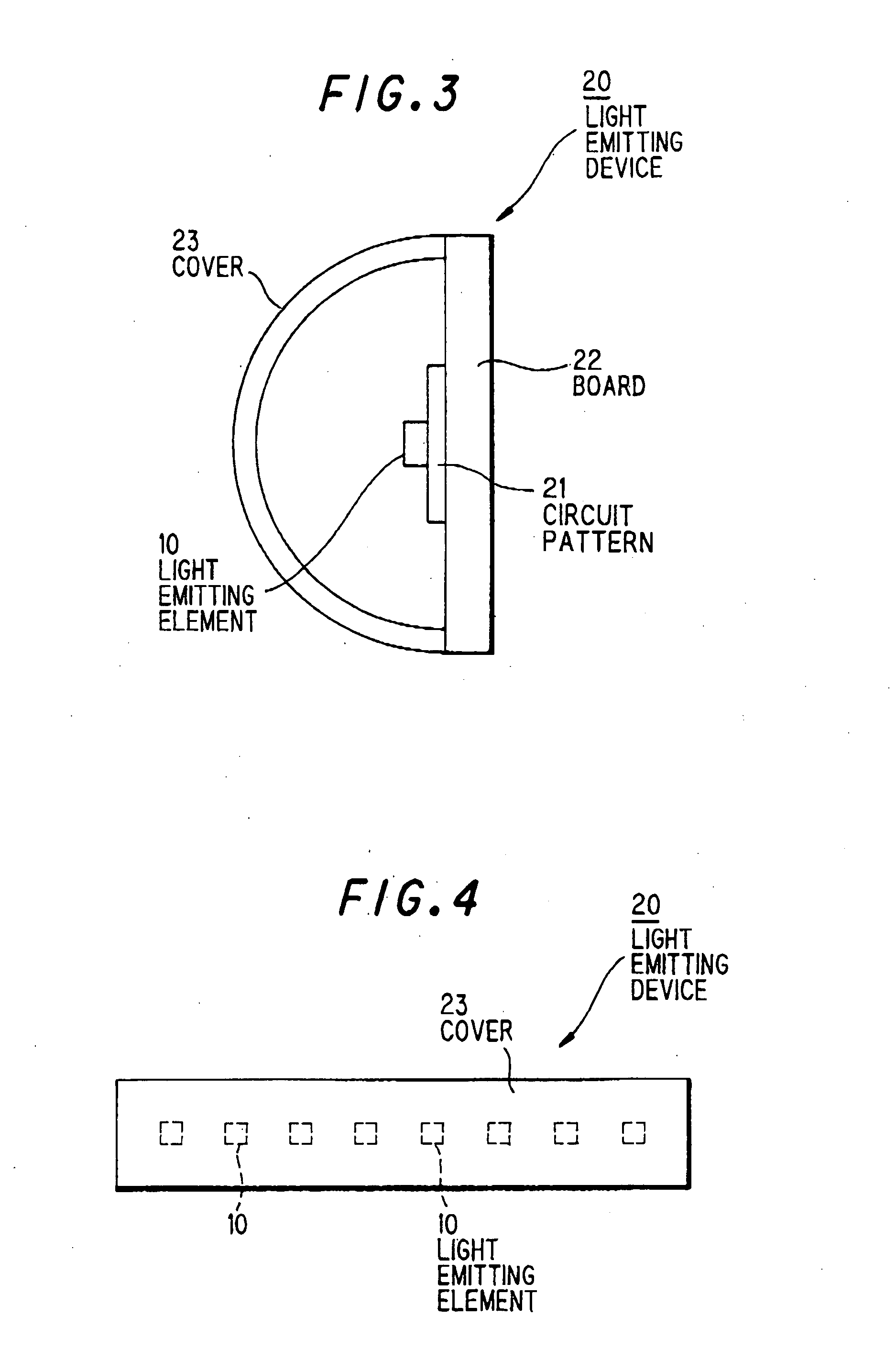
[0072] FIG. 5 is a side view showing a light emitting device 30 in the second preferred embodiment of the invention. Like components are indicated by the same numerals used in FIG. 3.

[0073] As shown in FIG. 5, the light emitting device 30 is provided with a cover 33 composed of three layers (phosphor layer). A first layer 33R on the outer surface is of fluorophosphate glass with Eu.sup.3+ doped therein (Lumilass R7 (registered trade mark): SUMITA Optical Glass, Inc.), a second layer 33G at the center is of fluorophosphate glass with Tb.sup.3+ doped therein (Lumilass G9(registered trade mark): SUMITA Optical Glass, Inc.), and a third layer 33B on the inner surface is of fluorophosphate glass with Eu.sup.2+ doped therein (Lumilass B(registered trade mark): SUMITA Optical Glass, Inc.). The layers 33R, 33G and 33B are to generate red-system fluorescence, green-system fluorescence and blue-system fluorescence, respectively. By mixing these three-color fluorescence lights, white-system li...

third embodiment

[0075] FIG. 6 is a cross sectional view showing a light emitting device 40 in the third preferred embodiment of the invention.

[0076] In the light emitting device 40, the light emitting element 10 is disposed at the bottom of a cup portion 42 of a mount lead 41. The cup portion 42 is filled with a phosphor layer 45, and the mount lead 41 and sub-lead 43 are sealed with a lamp-shaped seal member 47.

[0077] FIG. 7 is an enlarged cross sectional view showing the phosphor layer 45 and its vicinity in FIG. 6.

[0078] The phosphor layer 45 is composed of a transparent material 46 of epoxy resin etc. and ground phosphor glass particles 48, which are of fluorophosphate glass with Tb.sup.3+ doped therein (Lumilass G9(registered trade mark): SUMITA Optical Glass, Inc.), being dispersed in the transparent material 46. Since the phosphor glass has a specific density that is not significantly greater than that of a general phosphor material such as YAG system phosphor, it can be evenly dispersed in ...


PUM


Abstract

A light emitting device has a light emitting element, and a phosphor layer of phosphor glass to generate fluorescence while being excited by light emitted from the light emitting element. The light emitting element emits ultraviolet light, and the phosphor glass generates visible fluorescence while being excited by the ultraviolet light.

Description

[0001] The present application is based on Japanese patent application No. 2003-063016, the entire contents of which are incorporated herein by reference.[0002] 1. Field of the Invention[0003] This invention relates to a light emitting device and, particularly, to a light emitting device with a phosphor layer for wavelength-converting light emitted from a light emitting element.[0004] 2. Description of the Related Art[0005] Conventionally, a light emitting device is suggested that allows the wavelength conversion of light emitted from a light emitting element by a phosphor material to obtain a desired emission color.[0006] Such a light emitting device is, as shown in FIG. 1, composed of: a board 5; a circuit pattern 4 formed on the board 5; a light emitting element 1 mounted through the circuit pattern 4 on the board 5, the light emitting element 1 being enabled to emit ultraviolet light; a cover 2 that is formed semispherical while covering a light emitting element 1 to emit ultrav...

Claims


Application Information

Patent Timeline
Patent Type & Authority Applications(United States)
IPC IPC(8): H01L33/30H01L33/50H01L33/56H01L33/60H01L33/62
CPCH01L33/501H01L33/56H01L2224/48091H01L2224/48247H01L2924/00014H01L2224/48257H01L2224/8592H01L2924/181
Inventor SUEHIRO, YOSHINOBUINOUE, MITSUHIROKATO, HIDEAKITERAJIMA, TOHRUAIDA, KAZUYASAWANOBORI, NARUHITO
Owner TOYODA GOSEI CO LTD
Why Eureka
Try Eureka