Apparatus and method for optical interconnection

a technology of optical interconnection and apparatus, applied in the direction of optical elements, instruments, optical waveguide light guides, etc., can solve the problems of increasing loss of wiring, driving power disadvantage, crosstalk, etc., and achieve the effect of improving the efficiency of optical interconnection

Inactive Publication Date: 2004-10-21
IBM CORP
View PDF2 Cites 10 Cited by
  • Summary
  • Abstract
  • Description
  • Claims
  • Application Information

AI Technical Summary

Benefits of technology

[0020] With the unique and unobvious aspects of the invention, the present invention allows the electrical-optical-electrical transduction to be simplified enormously and provides high density (compared with other optical interconnects). Optical interconnects are normally less dense than conventional wires since bulky hybrid construction and elaborate laser driver and receiver circuitry is eliminated. Further, one laser source can be used commonly for illumination for a plurality of interconnects. Conventionally, a dedicated laser (and dedicated driver chip and dedicated photoreceiver at the other end) has been used for each line.
[0022] Another advantage of the invention is the extreme bandwidths (e.g., data has shown that the limit is higher than about 200 GHz) which are made possible, and near-zero latency. Such near-zero latency is provided since the signal need not go off the chip through a series of slow components (e.g. demultiplexers, long wires, etc.).
[0023] Further, the inventive structure can be manufactured entirely in monolithic silicon circuitry. Additionally, a great deal of power is saved over the conventional structures.
[0028] Further, the invention uses an antenna / tunnel junction combination as a waveguide detector. Additionally, the invention combines the antenna / tunnel junction combination as a waveguide detector into an optical interconnection system of extreme bandwidth, low power, high density, near-zero latency, and totally monolithic construction.

Problems solved by technology

The expense and difficulty of using these materials is more than repaid by the huge bandwidths and inter-repeater distances they allow.
However, as data rates increase, wiring will increasingly suffer loss, crosstalk, and drive power disadvantages.
However, the application is difficult for the optics since it requires high density, low cost, and extremely low latency (e.g., 100 picoseconds to a few nanoseconds).
The primary limiting factors on these short-range optical interconnections have been their high cost, large size, long latencies, and the drive power requirements of the current technologies.
The root of these problems is that there have been no monolithically integrated optical interconnection technologies.
The optoelectronic components (e.g., vertical-cavity surface emitting lasers (VCSELs), InGaAs photodiodes, etc.) cannot be made in silicon, and the laser driver chip must provide a 2-V output swing, which a processor working from a single 1-V supply cannot do without ancillary circuitry such as a charge pump.
Each of these components must be soldered or bonded on the board since lasers cannot be made of silicon.
This is problematic due to space, cost, and yield detraction.
A further problem of hybrid construction is that the logic signal must be transmitted electrically between the logic output and the laser or modulator.
If the laser or modulator is a separate chip, then this configuration requires the signal to be sent across an electrical transmission line on the module or circuit board, whose bandwidth and drive power requirements limit the benefit to be gained from the optical interconnection.
This relies on the inherent nonlinearity of the detector.
Because ordinary antennas must couple into free-space waves, such antennas are normally bilaterally symmetric, but as in the coaxial cable-to-metal-waveguide transition, an asymmetric structure may provide improved coupling into the lowest-order waveguide mode, especially since integrating metal elements into the core of the waveguide is difficult, and the coupling so achieved may be too strong, so that it is better to put the metal elements in the cladding region.

Method used


Image

  • Apparatus and method for optical interconnection
  • Apparatus and method for optical interconnection
  • Apparatus and method for optical interconnection

Examples


embodiment

PREFERRED EMBODIMENT

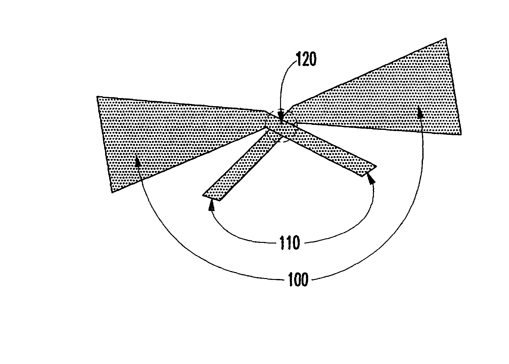
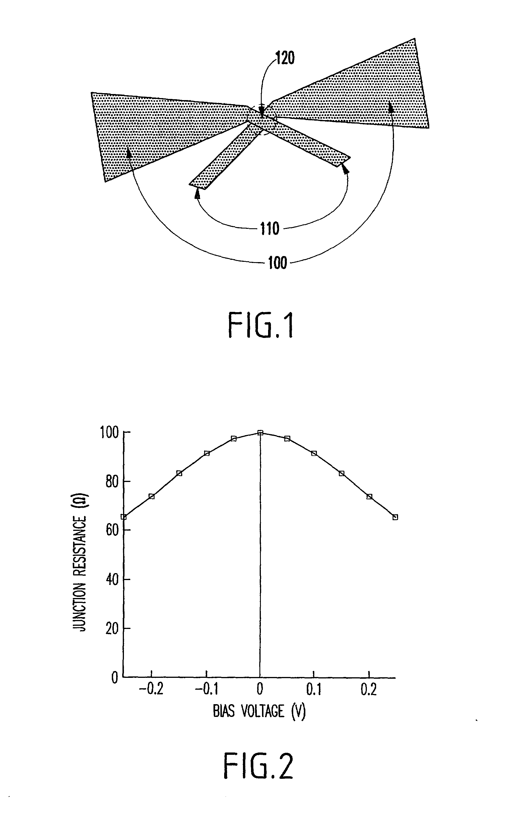
[0041] Turning now to FIG. 1, generally a dipole antenna 100 is shown including structures 110 for input / output of baseband signals and a tunnel junction 120 (e.g., formed of Ni--NiO--Ni, etc.).

[0042] The antenna 100 terminated in its characteristic impedance functions as an absorber with an effective cross-section much larger than its geometrical cross-sectional area. This allows the antenna 100 to be an efficient transducer of an incoming wave to an electrical signal at the antenna terminals.

[0043] In addition to the absorption, an antenna also scatters the incoming wave into other plane wave components. Such a small scatterer produces essentially a pure dipole pattern in the far field.

[0044] The optical theorem (also known as the "extinction sum rule") provides that the integral of the interference term between the light scattered by the dipole and the incident beam equals the total absorption plus the total scatter. This allows an estimate of the field scatte...


PUM


Abstract

An apparatus (and method) for launching a modulated optical signal, includes a waveguide, an antenna structure for communicating with the waveguide and with an externally-applied optical field and having an output port, and an electrically-variable-impedance device connected at the antenna's output port, capable of responding at a frequency of an externally-applied optical field and having its impedance at the optical frequency changed by an applied electrical signal.

Description

[0001] 1. Field of the Invention[0002] The present invention generally relates to a method and apparatus for optical interconnection and more particularly to a method and apparatus for optical interconnection in which an antenna is provided in a waveguide structure such that space and power are saved.[0003] 2. Description of the Related Art[0004] Long-haul, high speed data communications are currently handled almost exclusively by fiber optic transmission systems. These systems operate at wavelengths of about 1.3 microns to about 1.56 microns, where silica waveguides are highly transparent, because minimizing the optical loss is a key engineering requirement in such systems.[0005] Lasers and photodiodes at those wavelengths must be made of compound semiconductors such as indium-gallium arsenide (InGaAs) or the like. The expense and difficulty of using these materials is more than repaid by the huge bandwidths and inter-repeater distances they allow. Latencies in these networks are t...

Claims


Application Information

Patent Timeline
Patent Type & Authority Applications(United States)
IPC IPC(8): G02B6/12G02B6/42
CPCG02B6/4206G02B6/4214G02B2006/12142
Inventor HOBBS, PHILIP CHARLES DANBYMCGLASHAN-POWELL, MAURICE
Owner IBM CORP
Why Eureka
Try Eureka