Display device and display device driving method

a display device and driving method technology, applied in static indicating devices, solid-state devices, instruments, etc., can solve the problems of variable luminance increase in the complexity of a transistor circuit, and the capacity of an organic el element is much smaller than the one on the display screen, etc., to achieve stable display and simple driving principle

Active Publication Date: 2004-12-23
SOLAS OLED LTD
View PDF35 Cites 122 Cited by
  • Summary
  • Abstract
  • Description
  • Claims
  • Application Information

AI Technical Summary

Benefits of technology

[0006] It is an object of the present invention to provide a display device and a display device driving method, which allow stable display on the basis of a simple driving principle.
[0018] When a reset voltage is output to the plurality of signal lines within a period when none of the plurality of optical elements are selected, the signal lines reset charges stored in the preceding selection period. For this reason, the parasitic capacitance of the signal lines can be quickly charged within the next selection period so that even when a designation current having a smaller current value is supplied, the current value of the designation current can rapidly be set in the steady state. Hence, even an optical element such as an organic EL element whose luminance is modulated by a small current on the .mu.A order is allowed to quickly display multiple gray level luminances.

Problems solved by technology

However, the capacity of an organic EL element is much smaller than that of a liquid crystal element so a current flows to the organic EL element itself.
This leads to an increase in complexity of a circuit constituted by transistors.
It is therefore difficult to uniquely designate the current level to be supplied to an organic EL element on the basis of the gate voltage level of a switching transistor by changing the value of the voltage to be applied to the gate electrode of the transistor and thus changing the level of the current to be supplied to the organic EL element.
This may cause a variation in luminance on the display screen.

Method used


Image

  • Display device and display device driving method
  • Display device and display device driving method
  • Display device and display device driving method

Examples


second embodiment

[0113] An organic EL display according to the second embodiment will be described next.

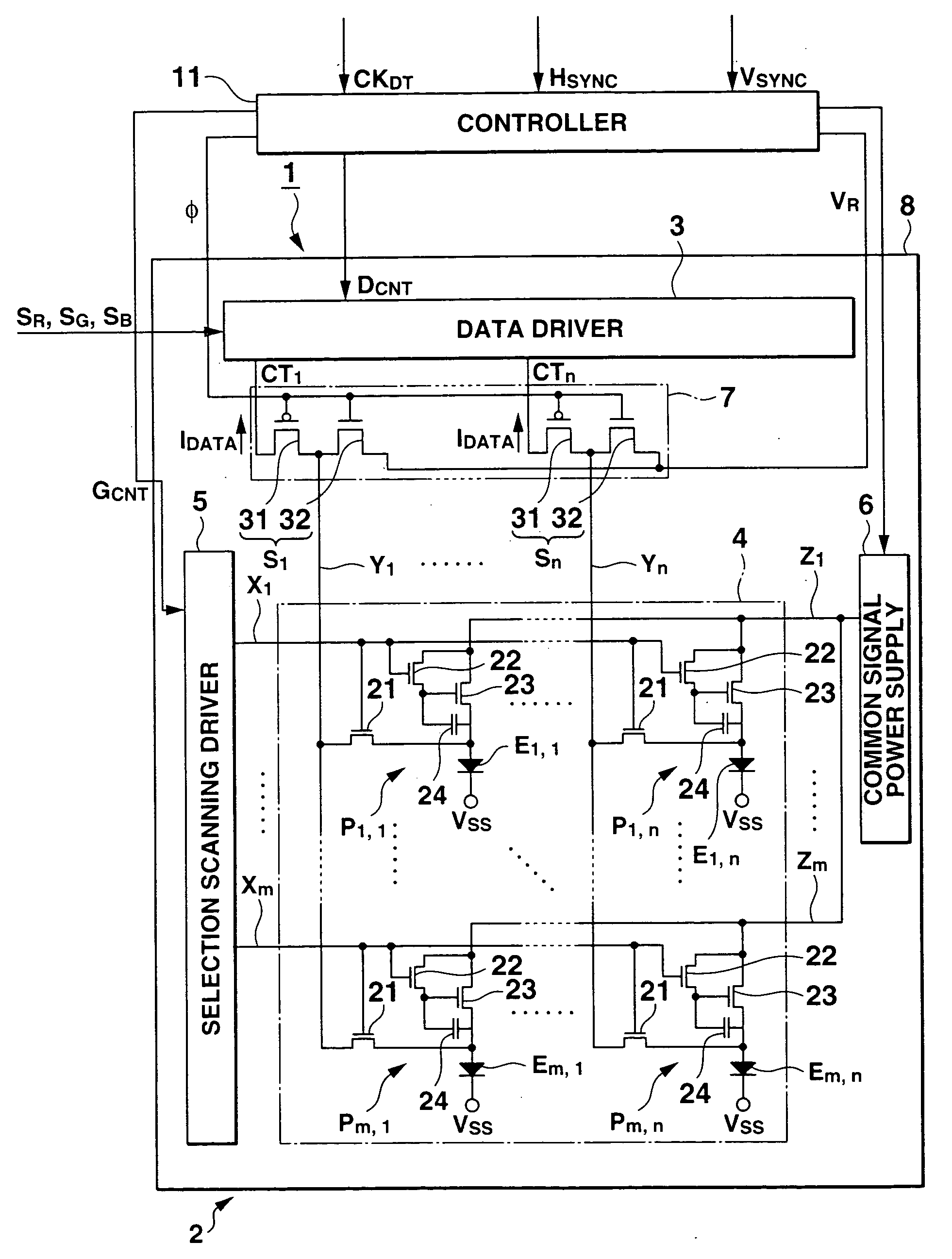
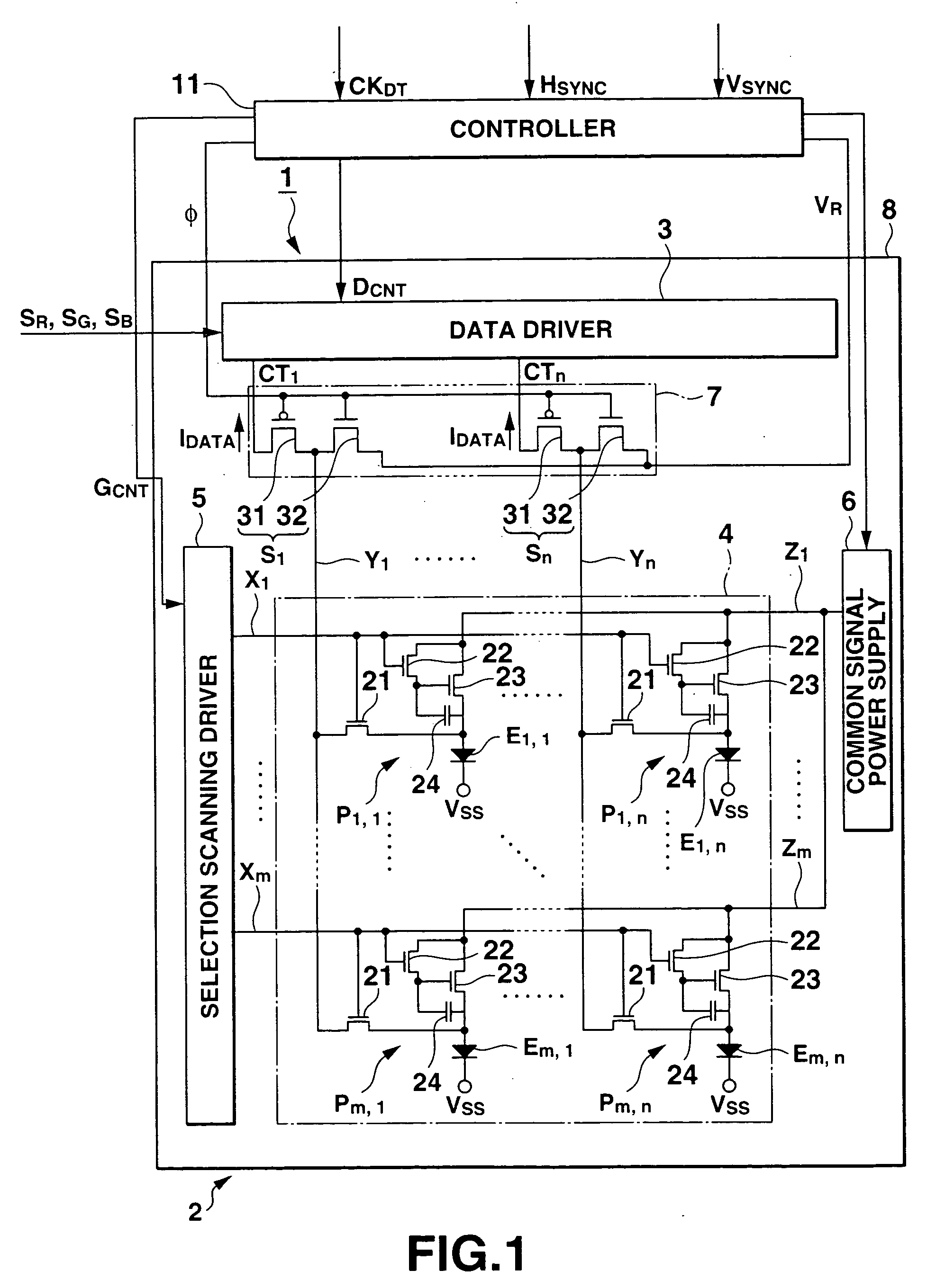
[0114] Even in the second embodiment, the organic EL display comprises an organic EL display panel 2, data driver 3, and selection scanning driver 5, like the organic EL display 1 according to the first embodiment shown in FIG. 1. The data driver 3, a display section 4, the selection scanning driver 5, pixel circuits D.sub.1,1 to D.sub.m,n, and light-emitting elements E.sub.1,1 to E.sub.m,n have the same structures as those in the organic EL display 1 of the first embodiment, and a detailed description thereof will be omitted in the second embodiment.

[0115] In the second embodiment, a common signal power supply 6 is arranged in a controller 11 connected to the organic EL display 1, as shown in FIG. 10. For this reason, the ratio of the occupied area of the pixels on the substrate of the organic EL display 1 can be increased.

[0116] The organic EL display 1 according to the second embodiment can ope...

third embodiment

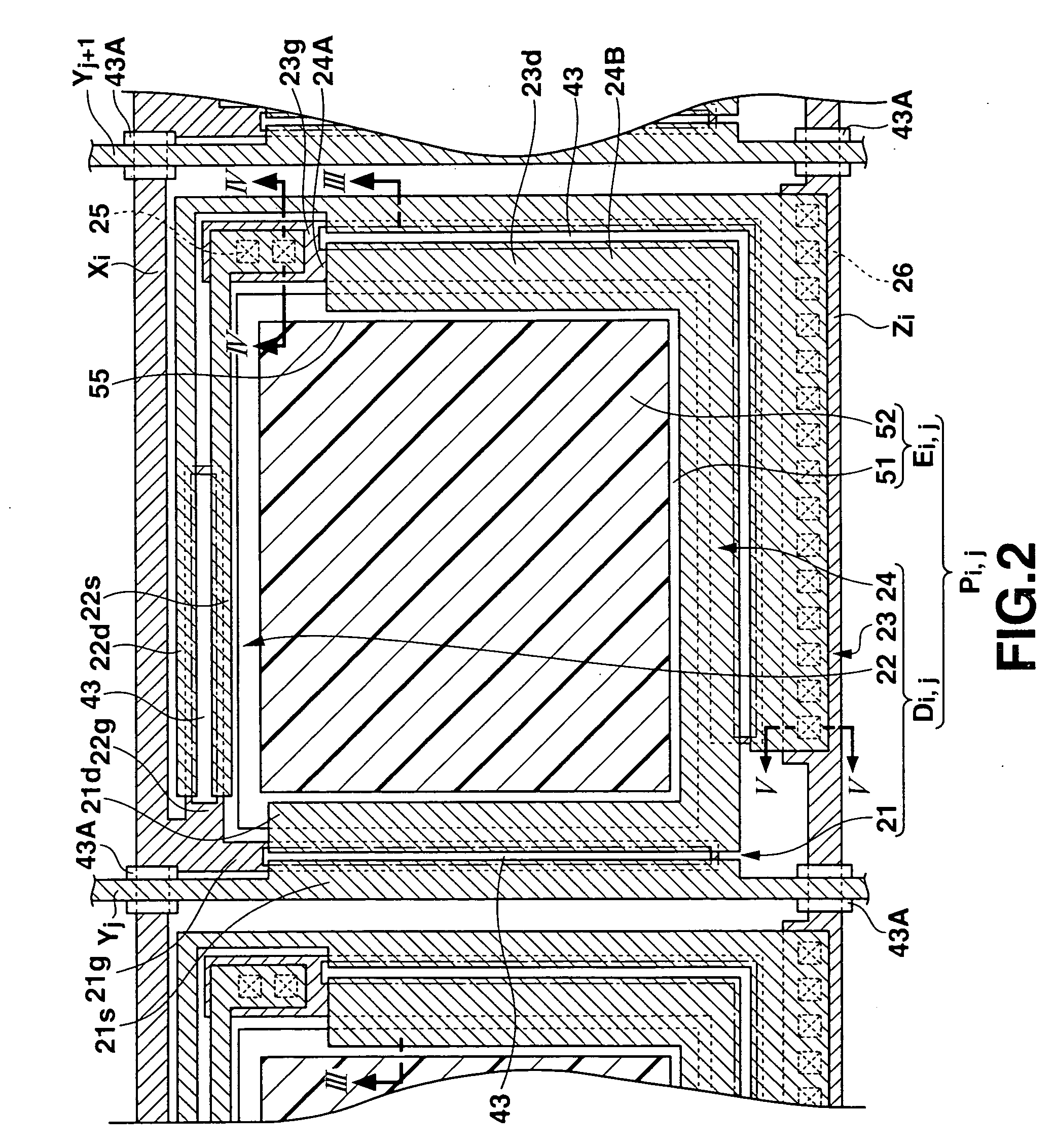
[0117] The third embodiment will be described next. This embodiment is the same as the first embodiment except that a drain 22d of a second transistor 22 of a pixel circuit D.sub.i,j of each pixel P.sub.i,j is not connected to a common signal supply line Z.sub.i but to a selection scanning line X.sub.i, as shown in FIG. 11. The same reference numerals as in the first embodiment denote the same parts in the third embodiment, and a detailed description thereof will be omitted.

[0118] In the transistor 22, the drain electrode 22d and gate electrode 22g are connected to the selection scanning line X.sub.i. A source electrode 22s is connected to a gate electrode 23g of a third transistor 23. The transistor 22 is an N-channel amorphous silicon thin film transistor, like a first transistor 21 and the transistor 23.

[0119] The transistor 22 operates upon receiving the voltage shown in the waveform chart in FIG. 8. That is, as shown in FIG. 12A, during a selection period T.sub.SE, the transist...


PUM


Abstract

A display device includes a plurality of scanning lines (X1-Xm), a plurality of signal lines (Y1-Yn), a scanning driver (5) which sequentially supplies to the scanning lines selection signals that select the scanning lines, a data driver (3) which supplies a designation current to the plurality of signal lines within a selection period when the scanning lines are being selected, a plurality of pixel circuits which supplies a driving current corresponding to a current value of the designation current that flows to the signal lines, a plurality of optical elements (E1,1-Em,n) which emit light in accordance with the driving current supplied by the plurality of pixel is circuits and a power supply (6) which outputs to the plurality of pixel circuits a driving current reference voltage to supply the driving current.

Description

[0001] The present invention relates to a display device and a display device driving method.[0002] Liquid crystal displays are generally classified into active matrix driving liquid crystal displays and simple matrix driving liquid crystal displays. The active matrix driving liquid crystal display displays an image having a higher luminance, higher contrast, and higher resolution as compared to the simple matrix driving liquid crystal display. In the active matrix driving liquid crystal display, a liquid crystal element which also functions as a capacitor and a transistor which activates the liquid crystal element are arranged for each pixel. In the active matrix driving liquid crystal display, a selection signal is input from a scanning driver serving as a shift register to a scanning line so that the scanning line is selected. At this time, when a voltage having a level representing a luminance is applied from a data driver to a signal line, the voltage is applied to the liquid c...

Claims


Application Information

Patent Timeline
Patent Type & Authority Applications(United States)
IPC IPC(8): G09G3/20G09G3/32G09G3/30H01L27/32
CPCG09G3/2011G09G3/325G09G3/3283G09G2300/0408G09G2300/0842H01L27/3244G09G2310/0248G09G2310/0251G09G2310/0256G09G2310/0297G09G2310/066G09G2300/0866H10K59/12G09G3/30
Inventor YAMADA, HIROYASUSHIRASAKI, TOMOYUKI
Owner SOLAS OLED LTD
Why Eureka
Try Eureka