Arrangement and method for digital delay line

a technology of digital delay and arrangement method, applied in the direction of oscillator generator, pulse generation by logic circuit, pulse technique, etc., can solve the problems of large silicon area of integrated circuit, large silicon area of digital delay line with high resolution, signal to be delayed is distorted

Active Publication Date: 2004-12-30
NXP USA INC
View PDF10 Cites 14 Cited by
  • Summary
  • Abstract
  • Description
  • Claims
  • Application Information

AI Technical Summary

Problems solved by technology

However, this approach has the disadvantage(s) that traditionally a digital delay line with high resolution and long delay occupies a big silicon area of an integrated circuit.
In addition, the signal to be delayed is distorted as more as the delay line becomes longer.

Method used


Image

  • Arrangement and method for digital delay line
  • Arrangement and method for digital delay line

Examples


Embodiment Construction

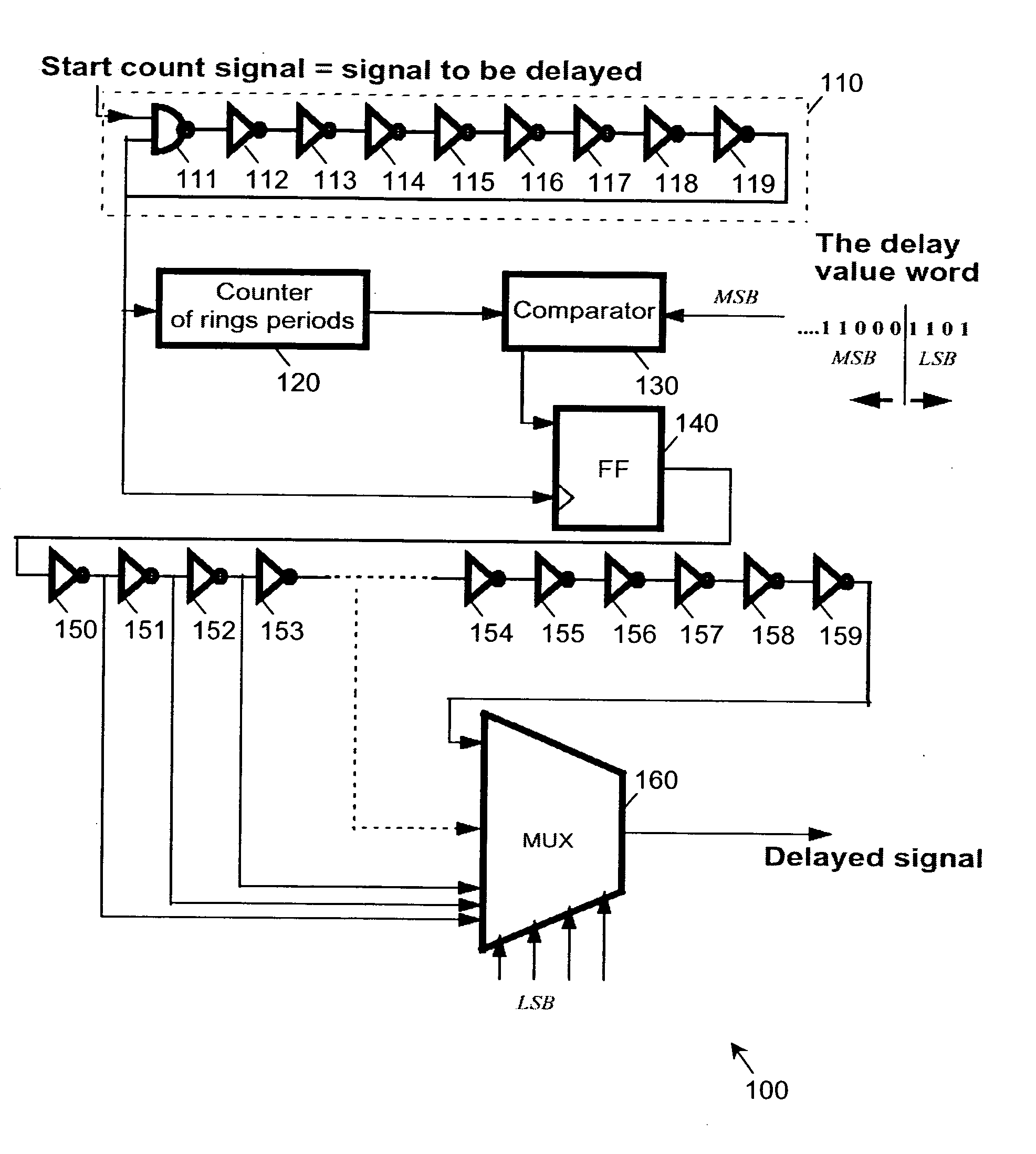
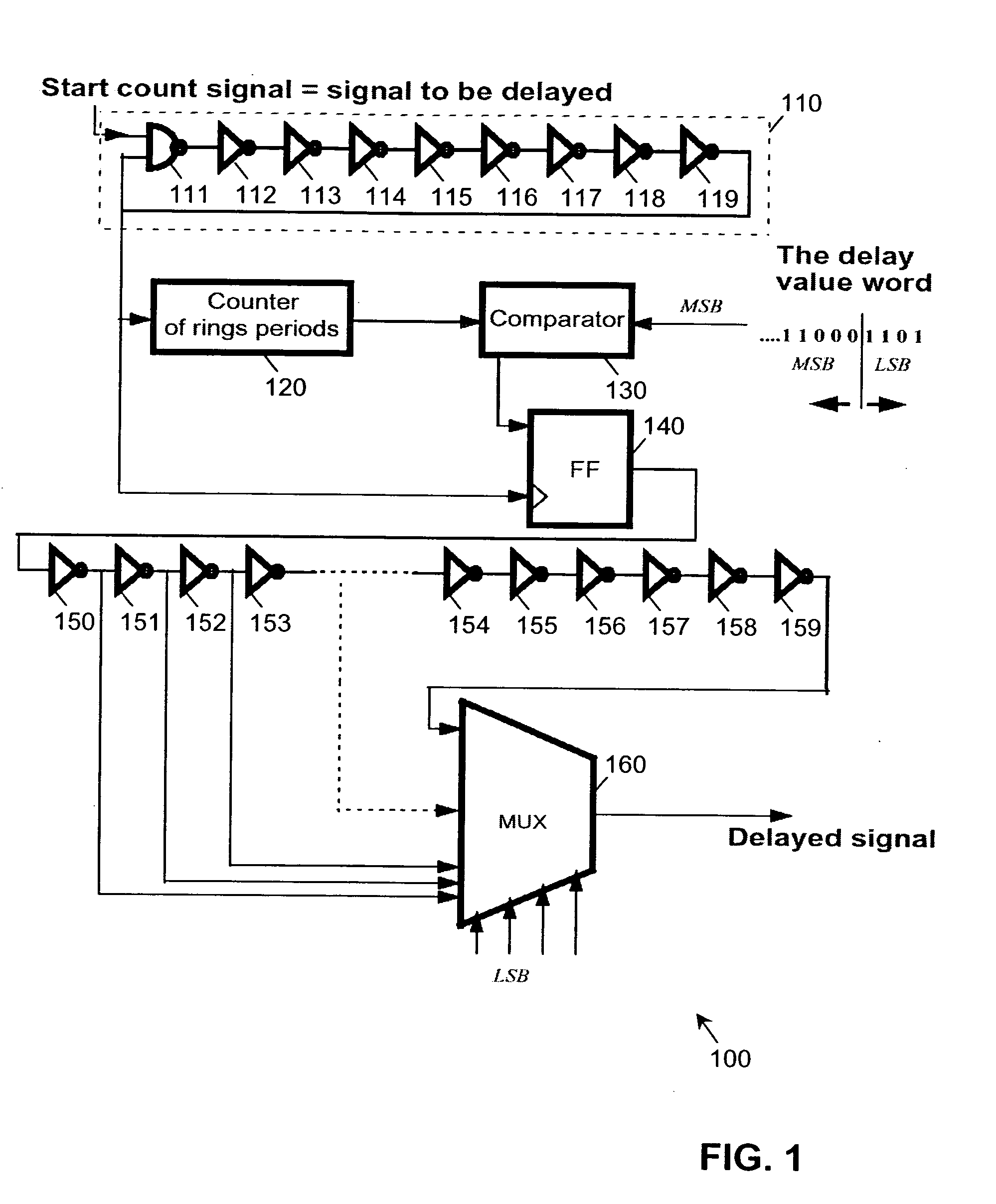
[0009] The infinite delay, high precision and low distortion digital delay line arrangement 100 includes a ring oscillator 110 constituted by an inverting AND gate 111 having an input for receiving a start count signal, i.e., the signal to be delayed. The output of the AND gate 111 is connected to a serially-coupled line of inverters 112-119, the output of the inverter 119 being connected to another input of the AND gate 111 and to the output of the oscillator.

[0010] The output of the oscillator is connected to a counter 120. The output of the counter is connected to an input of a comparator 130, of which another input is arranged to receive the most significant bits (MSB) of a binary word constituting the delay value. The output of the comparator 130 is connected to the data input of a flip-flop 140, whose clock input is connected to the output of the oscillator 110.

[0011] The output of the flip-flop 140 is connected to a line of serially coupled inverters, of which ten (150-153 an...


PUM


Abstract

An arrangement (100) and method for a high precision and low distortion digital delay line with infinite delay. The digital delay line has an oscillating ring (110) with an odd number of inverting elements that triggers a counter (120). A comparator (130) compares the counter and the MSB of a given delay word. A line of inverters (150-159), double the odd number in the ring oscillator, is connected to a MUX (160) controlled by the LSB of the delay word. This provides the advantages of: high resolution due to use of a small, basic component, self-delay ring oscillator; small silicon area due to use of a special decoding scheme use the rings number to produce large delays; and easy implementation as a digital block in an integrated circuit using a standard cells library to build the ring and the decoder.

Description

[0001] This invention relates to digital delay lines, and particularly (though not exclusively) to digital delay lines which provide long (commonly termed `infinite`) delay while maintaining high delay resolution and low distortion.[0002] In the field of this invention it is known that typically in a digital delay line the signal to be delayed is propagated through a line of inverters and a multiplexer (MUX) to select the location (inverter) at which the signal will be output.[0003] However, this approach has the disadvantage(s) that traditionally a digital delay line with high resolution and long delay occupies a big silicon area of an integrated circuit. In order to build a long digital delay line with small silicon area, the resolution must be decreased. In addition, the signal to be delayed is distorted as more as the delay line becomes longer.[0004] A need therefore exists for an arrangement and method for a digital delay line with infinite delay wherein the abovementioned disa...

Claims


Application Information

Patent Timeline
Patent Type & Authority Applications(United States)
IPC IPC(8): H03B1/00H03K5/00H03K5/13
CPCH03K2005/00156H03K5/133H03K2005/00247
Inventor ROSENBAUM, YAIRSADE, SHAISOFER, SERGEYYEHUSHUA, EMIL
Owner NXP USA INC
Why Eureka
Try Eureka