
Method and apparatus for electrochemical mechanical processing

a mechanical processing and electrochemical technology, applied in the direction of manufacturing tools, abrasive surface conditioning devices, lapping machines, etc., can solve the problems of difficult to remove all copper residues, difficult to perform bulk and residual material removal at a single polishing station,

Inactive Publication Date: 2005-01-06
APPLIED MATERIALS INC
View PDF99 Cites 74 Cited by
  • Summary
  • Abstract
  • Description
  • Claims
  • Application Information

AI Technical Summary

Problems solved by technology

However, the removal of copper residue may result in dishing of copper features below the plane of a surrounding material, typically an oxide Or a barrier layer of other materials, such as TaN, and the like.
As the copper layer does not have a uniform thickness across the substrate, it is difficult to remove all the copper residue without causing dishing over some features and not removing all of the copper residue over others.
However, at the present time, it is difficult to perform both bulk and residual material removal at a single polishing station.

Method used


Image

  • Method and apparatus for electrochemical mechanical processing
  • Method and apparatus for electrochemical mechanical processing
  • Method and apparatus for electrochemical mechanical processing

Examples


Embodiment Construction

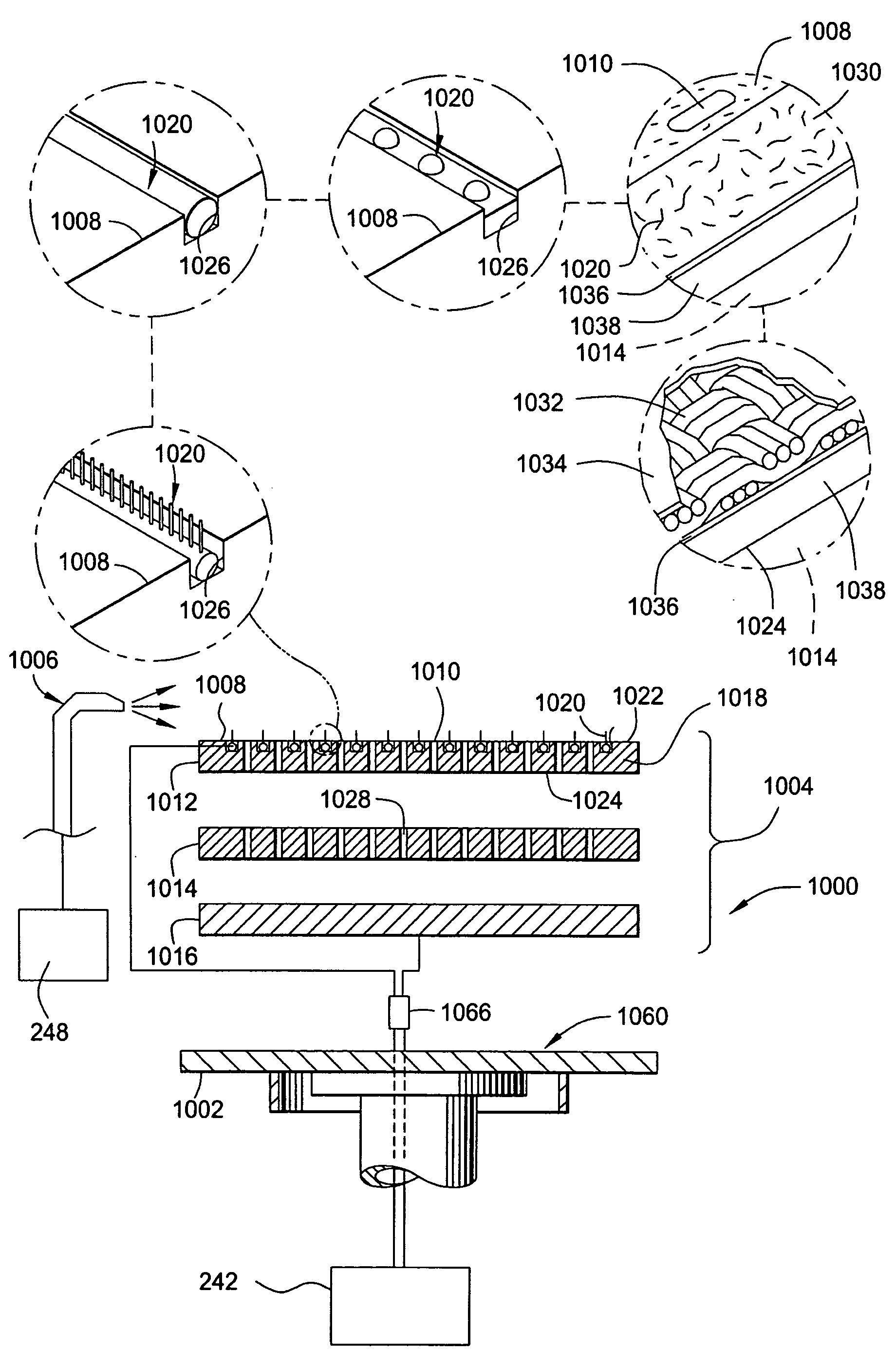
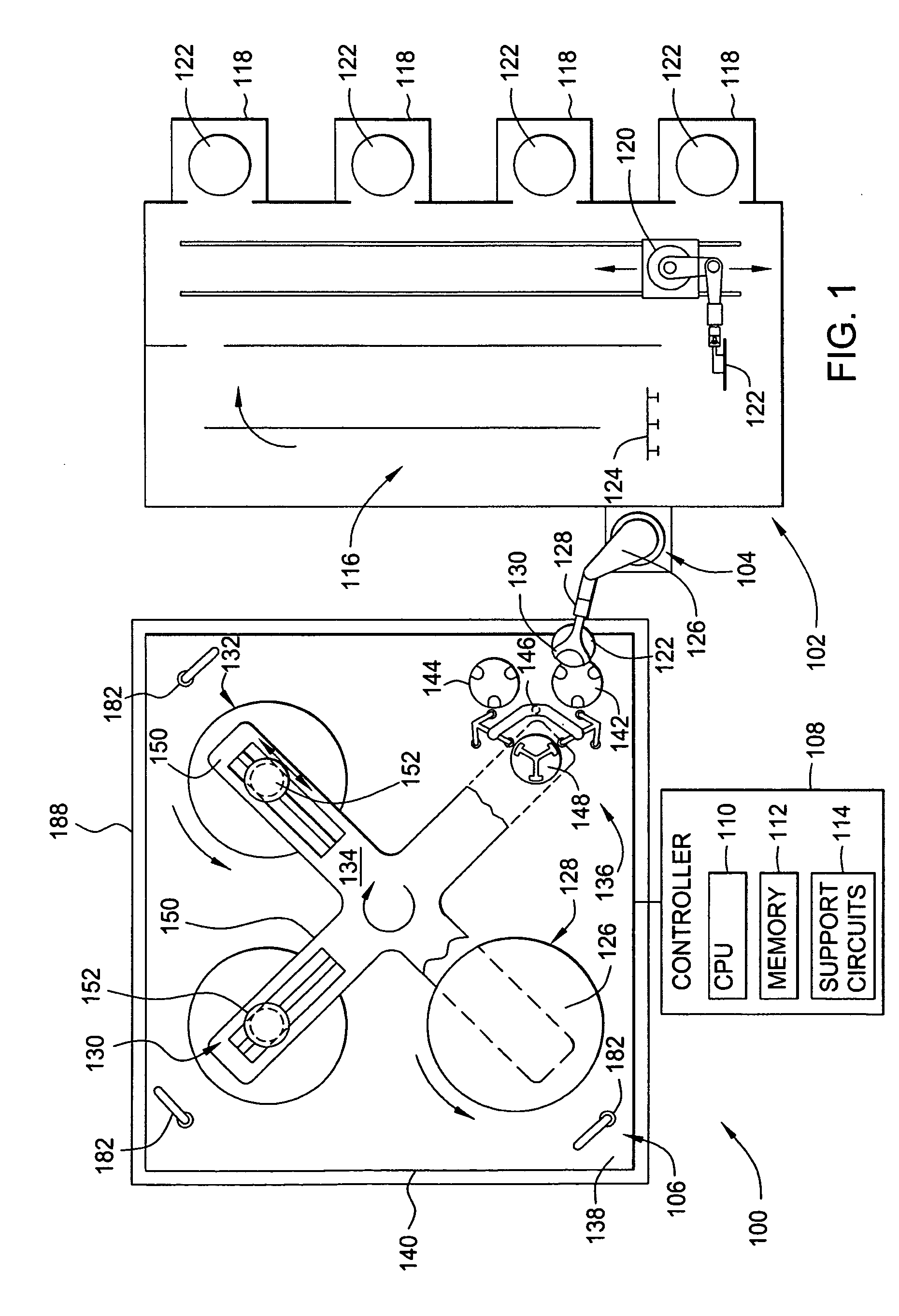
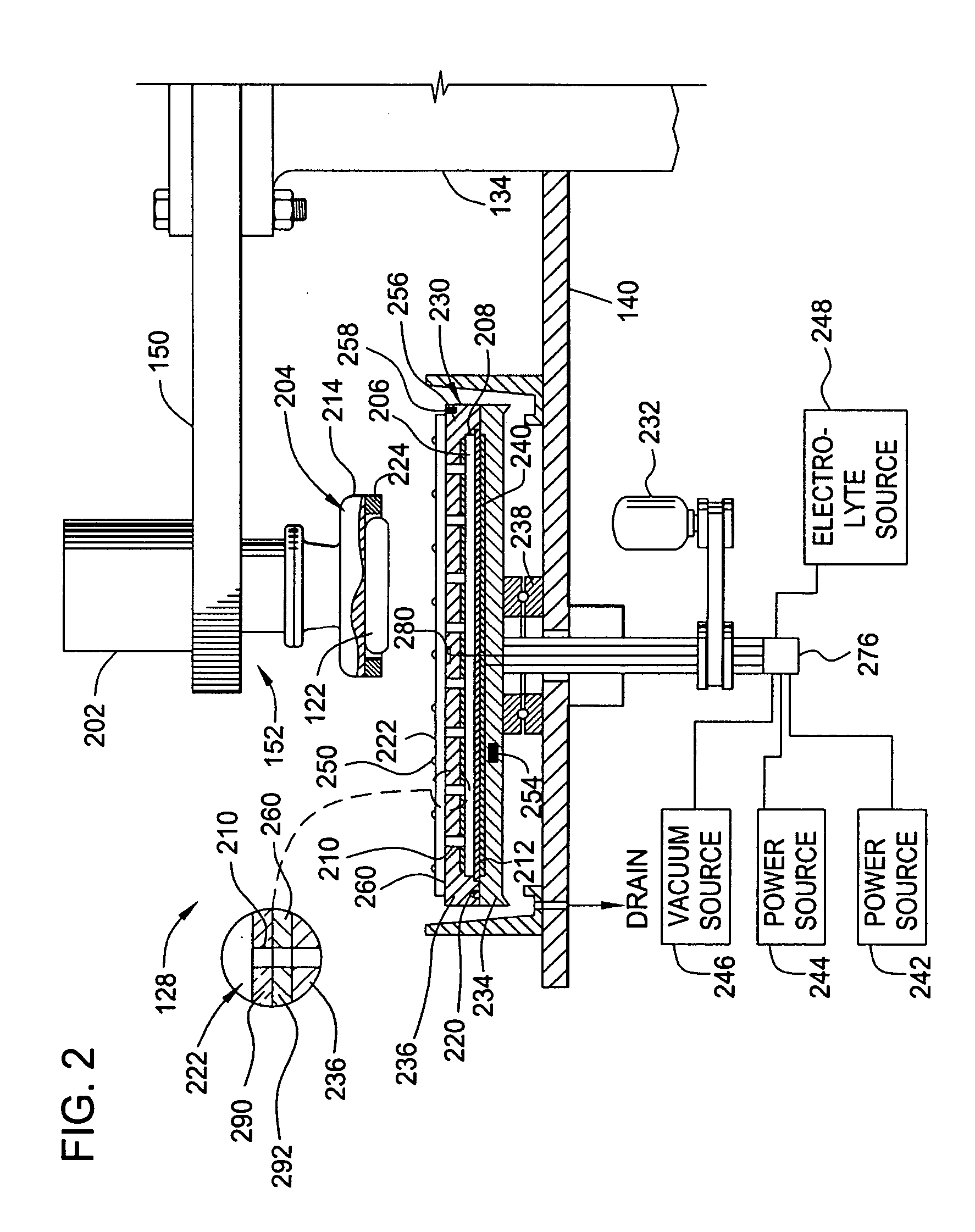
[0028] Embodiments for a system and method for the bulk and residual removal of conductive material from a substrate is provided. Although the system is illustratively described having at least two processing stations suitable for the removal of conductive material disposed around a central substrate transfer device, it is contemplated that the inventive processing stations may be arranged in other configurations, and / or be supplied substrates by other types or configurations of substrate transfer mechanisms. Furthermore, although the embodiments disclosed below focus primarily on removing material from, e.g., planarizing, a substrate, it is contemplated that the teachings disclosed herein may be used to electroplate a substrate by reversing the polarity of the bias.

[0029]FIG. 1 is a plan view of one embodiment of a planarization system 100 having an apparatus for electrochemically processing a substrate. The exemplary system 100 generally comprises a factory interface 102, a loadi...


PUM

PropertyMeasurementUnit
thickaaaaaaaaaa
conductiveaaaaaaaaaa
electrically biasaaaaaaaaaa

Abstract

Embodiments of the invention generally provide a method and apparatus for processing a substrate in an electrochemical mechanical planarizing system. In one embodiment, a cell for polishing a substrate includes a processing pad disposed on a top surface of a platen assembly. A plurality of conductive elements are arranged in a spaced-apart relation across the upper planarizing surface and adapted to bias the substrate relative to an electrode disposed between the pad and the platen assembly. A plurality of passages are formed through the platen assembly between the top surface and a plenum defined within the platen assembly. In another embodiment, a system is provided having a bulk processing cell and a residual processing cell. The residual processing cell includes a biased conductive planarizing surface. In further embodiments, the conductive element is protected from attack by process chemistries.

Description

CROSS-REFERENCE TO RELATED APPLICATIONS [0001] This application claims benefit of U.S. Provisional Patent Application Ser. No. 60 / 484,189 (Attorney Docket No. 4100L), filed Jul. 1, 2003, and U.S. Provisional Patent Application Ser. No. 60 / 516,680 (Attorney Docket No. 4100L02), filed Nov. 3, 2003, both of which are herein incorporated by reference. This application is additionally a continuation-in-part of co-pending U.S. patent application Ser. No. 10 / 608,513 (Attorney Docket No. 4100P7), filed Jun. 26, 2003 (hereinafter referred to as the “'513 application”), which is a continuation-in-part of co-pending U.S. patent application Ser. No. 10 / 140,010 (Attorney Docket No. 7047), filed May 7, 2002. The '513 application is also a continuation-in-part of co-pending U.S. patent application Ser. No. 10 / 211,626 (Attorney Docket No. 4100P3), filed Aug. 2, 2002, which is a continuation-in-part of co-pending U.S. patent application Ser. No. 10 / 033,732 (Attorney Docket No. 4100P1, renumbered 410...

Claims


Application Information

Patent Timeline
Patent Type & Authority Applications(United States)
IPC IPC(8): B23H5/06B23H5/08B23H5/10B24B37/04B24B49/16B24B53/007B24D13/14H01L21/321
CPCB23H5/06B23H5/08B23H5/10H01L21/32125B24B37/16B24B49/16B24B53/017B24B37/046
Inventor WANG, YANNEO, SIEWLIU, FENGTSAI, STAN D.HU, YONGQIDUBOUST, ALAINMANENS, ANTOINEWADENSWEILER, RALPH M.MAVLIEV, RASHIDCHEN, LIANG-YUHOLGADO, DONALD J.K.BUTTERFIELD, PAUL D.TSENG, MING-KUEICHANG, SHOU-SUNGSUN, LIZHONG
Owner APPLIED MATERIALS INC
Learn More