Method of fabricating and architecture for vertical transistor cells and transistor-controlled memory cells

a technology of vertical transistor cells and memory cells, applied in the direction of transistors, electrical devices, semiconductor devices, etc., can solve the problems of affecting altering the electrical properties of the transistor cell, and affecting the functional restriction of the transistor cell by a floating body effect, so as to increase the area requirement and reduce the functional restriction of the transistor cell

Inactive Publication Date: 2005-01-06
POLARIS INNOVATIONS LTD
View PDF14 Cites 208 Cited by
  • Summary
  • Abstract
  • Description
  • Claims
  • Application Information

AI Technical Summary

Benefits of technology

[0011] Embodiments of the present invention provide for a transistor cell architecture and memory cell architecture in which a functional restriction of the transistor cells by a floating body effect is reduced without increasing an area requirement significantly, with respect to conventional memory cell concepts for 4 F2 or 8 F2 transistor cells or 4 F2 or 8 F2 memory cells. Further embodiments include a method for fabricating such a transistor cell or memory cell.

Problems solved by technology

A disadvantage of the illustrated architecture of transistor cells 81 is that active regions 3 of transistor cells 81 are electrically without connection.
However, an accumulation of majority carriers in the active region disadvantageously alters the electrical properties of the transistor cell.
As a result, a charge stored on the storage capacitor is altered and a datum represented by the charge and stored in the memory cell is corrupted, if the storage capacitor is not recharged within a specified time.
Each recharging process increases an average access time to the datum stored in the memory cell and the power consumption of the memory cell.

Method used


Image

  • Method of fabricating and architecture for vertical transistor cells and transistor-controlled memory cells
  • Method of fabricating and architecture for vertical transistor cells and transistor-controlled memory cells
  • Method of fabricating and architecture for vertical transistor cells and transistor-controlled memory cells

Examples


Embodiment Construction

[0035] The following list of reference symbols is used consistently in the discussion to follow.
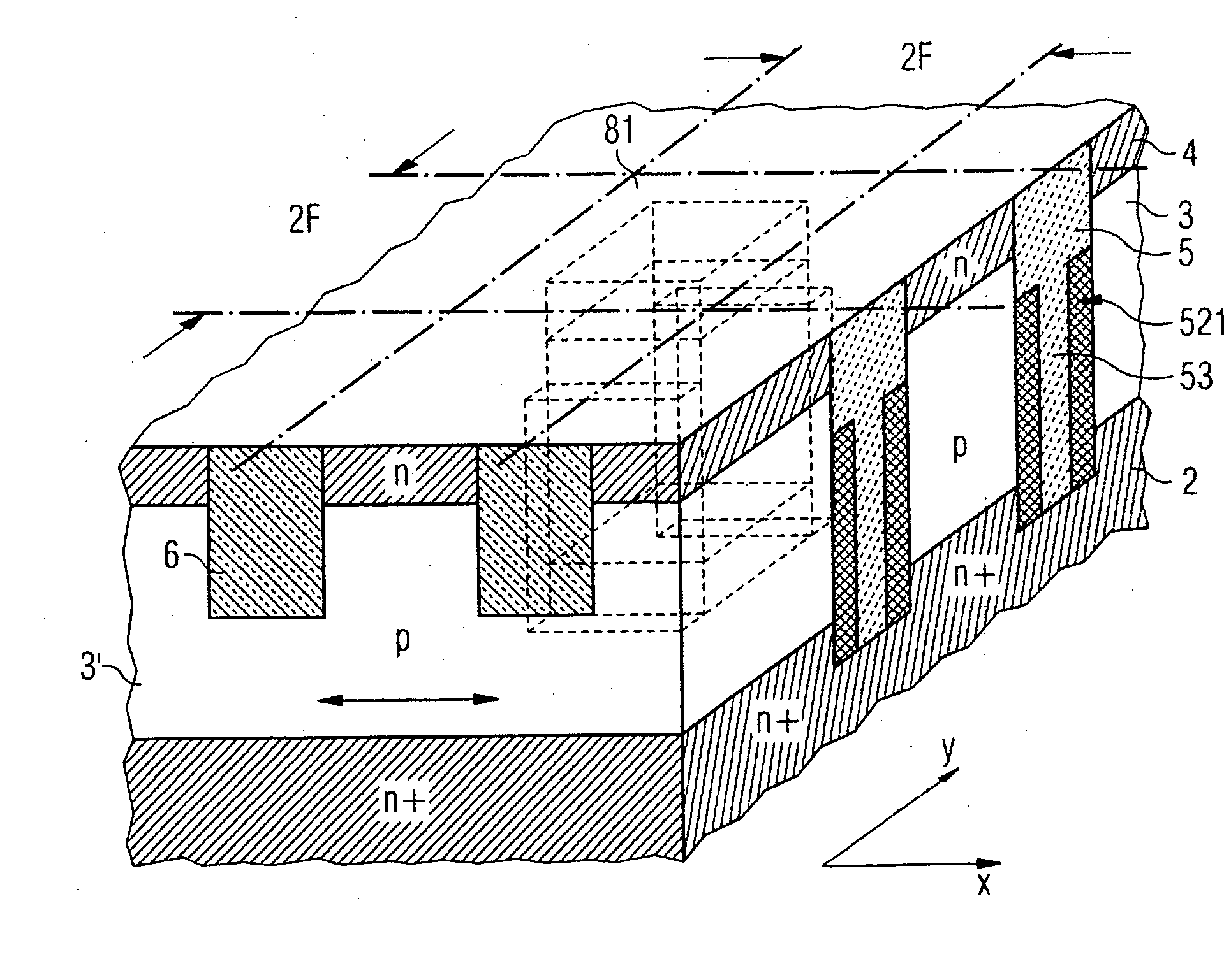
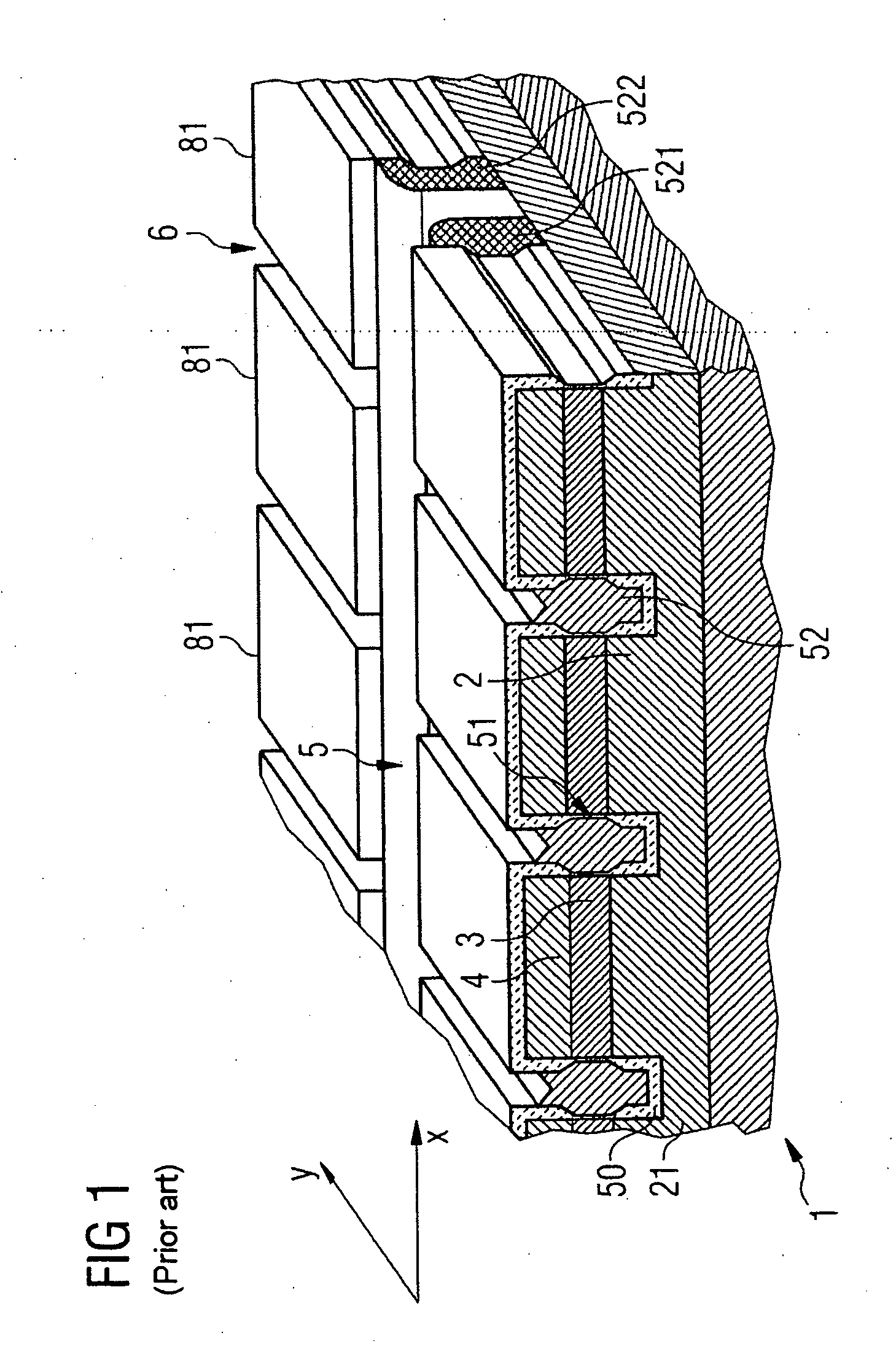
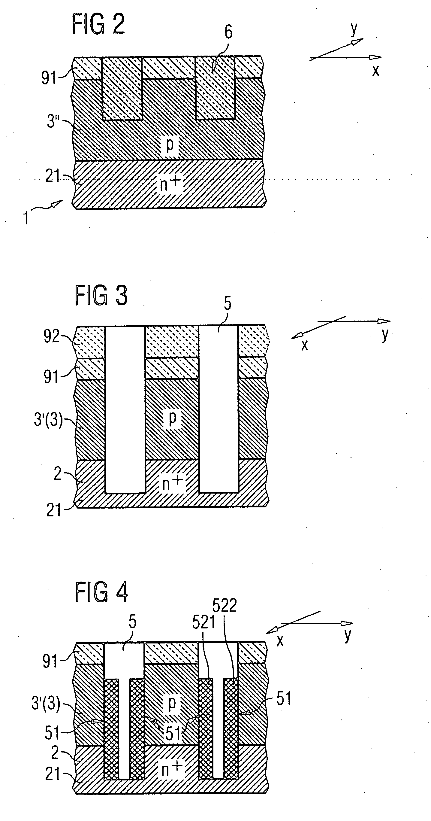
[0036]1 Substrate

[0037]2 Lower source / drain connection region

[0038]21 Connection plate (buried layer)

[0039]3 Active region

[0040]3′ Layer body

[0041]3″ Precursor layer body

[0042]31 First epitaxial layer

[0043]32 Second epitaxial layer

[0044]33 Transistor web

[0045]4 Upper source / drain connection region

[0046]4′ Preliminary stage of the upper source / drain connection region

[0047]5 Active trench

[0048]50 Insulator layer

[0049]51 Gate dielectric

[0050]52 Gate electrode

[0051]521, 522 Word line

[0052]53 Word line insulator (inter wordline fill)

[0053]6 Isolation trench

[0054]71 Process layer

[0055]81 Transistor cell (selection transistor)

[0056]82 Storage capacitor

[0057]91 Working layer

[0058]92 Mask

[0059] FIGS. 2 to 7 illustrate the fabrication of a transistor cell architecture according to a first exemplary embodiment of the present invention at various steps, using cross sections an...


PUM


Abstract

In a substrate vertical transistor cells are formed and are arranged, in a transistor cell array, row by row in an x direction and column by column in a y direction. Lower source/drain regions of the transistor cells are connected to a common connection plate. Upper source/drain regions of the transistor cells impart a contact connection for instance to a storage capacitor of a DRAM memory cell. Active trenches running between the transistor cells with word lines are formed along the x direction. The word lines form gate electrodes in sections. A potential at the gate electrode controls a conductive channel in an active region arranged in each case between the upper and the lower source/drain connection region. According to the invention, the active regions of adjacent transistor cells are sections of a contiguous layer body and are connected to one another. An accumulation of charge carriers in the active region and floating body effects are avoided without increasing the area requirement of a transistor cell.

Description

BACKGROUND [0001] 1. Field of the Invention [0002] The present invention relates generally to semiconductor devices and in particular to semiconductor memory architecture. [0003] 2. Background of the Invention [0004] Memory cells of dynamic random access memories (DRAMs) are usually designed as one transistor / one capacitor (ITIC) memory cells each having a storage capacitor for storing charge carriers and a selection transistor for addressing the storage capacitor. In the case of memory cells of the “trench capacitor” type, the storage capacitors are arranged in the substrate essentially below a transistor plane formed by the selection transistors and, in the case of memory cells of the “stacked capacitor” type, essentially above the transistor plane. [0005] To increase the performance of DRAMs, both miniaturization of the feature sizes and achieving a smallest possible spacing between memory cells relative to a minimum feature size F is desirable. The minimum feature size may be re...

Claims


Application Information

Patent Timeline
Patent Type & Authority Applications(United States)
IPC IPC(8): H01L21/8239H01L21/8242H01L27/105H01L27/108
CPCH01L27/10876H01L27/10823H10B12/34H10B12/053H10B12/00
Inventor SCHLOESSER, TILLMANGER, DIRKGOEBEL, BERND
Owner POLARIS INNOVATIONS LTD
Why Eureka
Try Eureka