Barrier metal layer for a carbon nanotube flat panel display

a carbon nanotube and flat panel display technology, applied in the manufacture of discharge tube main electrodes, discharge tube/lamp manufacture, electrode systems, etc., can solve the problems of poor yield, high cost, large and bulky prior art crt displays, etc., and achieve the effect of not increasing the number of masking steps

Inactive Publication Date: 2005-01-06
ARROW CAPITAL +1
View PDF16 Cites 14 Cited by
  • Summary
  • Abstract
  • Description
  • Claims
  • Application Information

AI Technical Summary

Benefits of technology

[0029] In some embodiments for making the electron-emitting device, a method for making the device may eliminate the need for an extra masking step to provide an in

Problems solved by technology

However, prior art CRT displays are large and bulky due to the large vacuum envelopes that enclose the cathode and extend from the cathode to the faceplate of the display.
This size limits the number of tips per pixel possible for high-resolution displays, where large numbers (400-1000 emitters per pixel) are desirable for uniform emission to provide adequate gray levels, and to reduce the current density per tip for s

Method used


Image

  • Barrier metal layer for a carbon nanotube flat panel display
  • Barrier metal layer for a carbon nanotube flat panel display
  • Barrier metal layer for a carbon nanotube flat panel display

Examples


Embodiment Construction

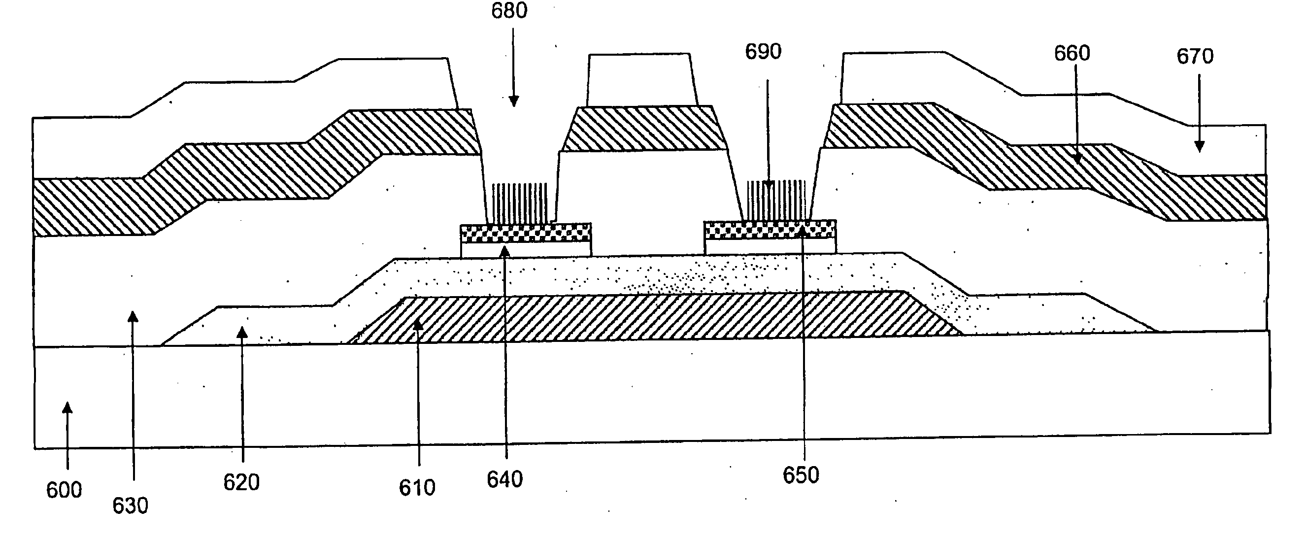
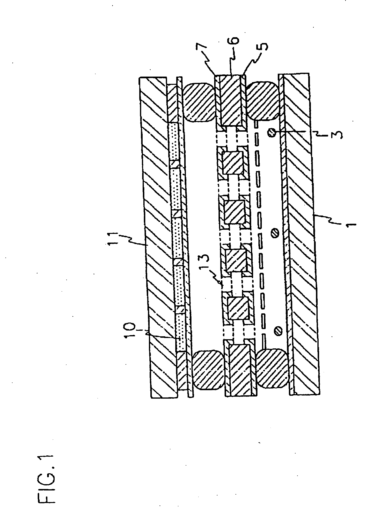
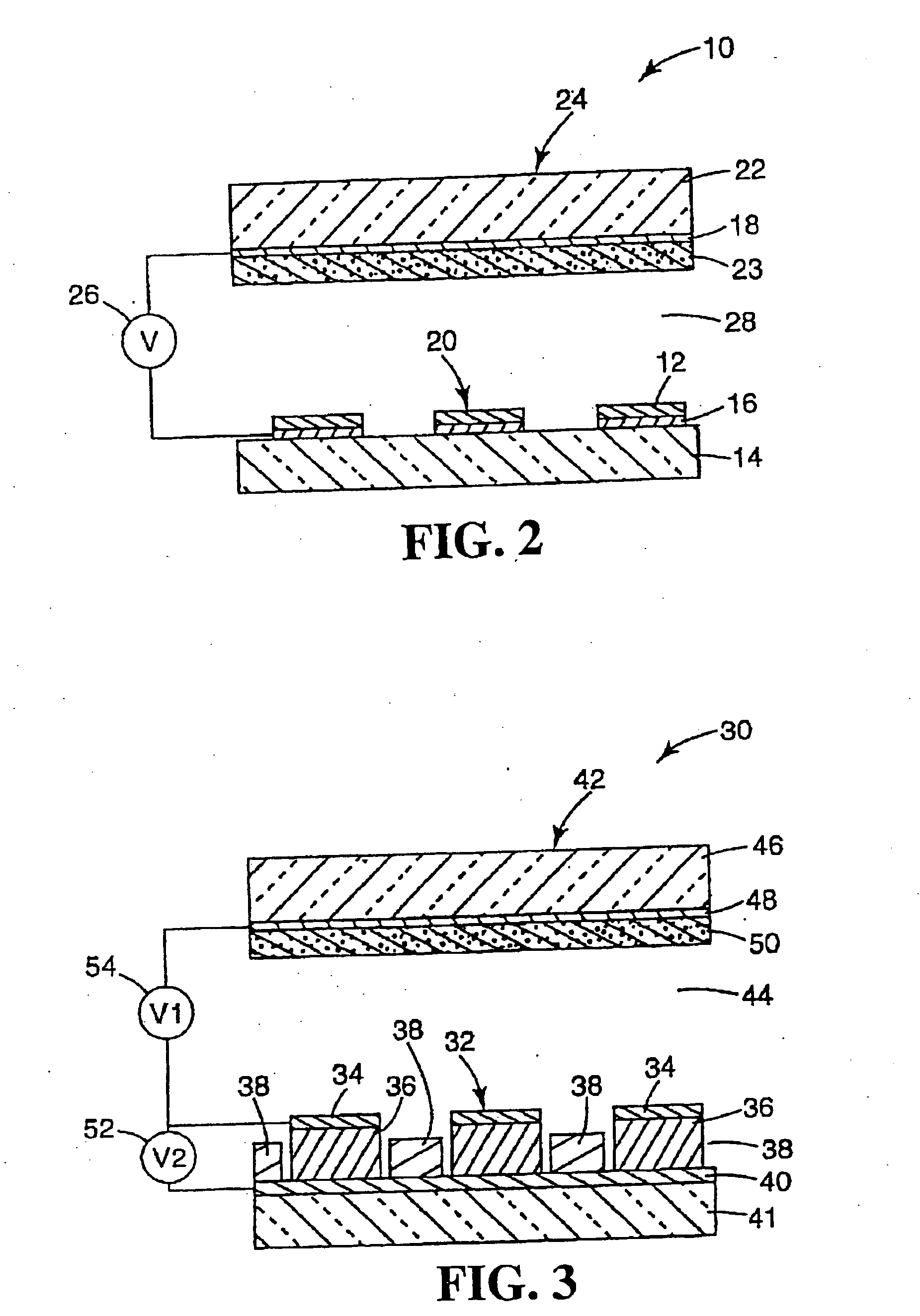
[0037] Reference will now be made in detail to the preferred embodiments of the invention, examples of which are illustrated in the accompanying drawings. While the invention will be described in conjunction with the preferred embodiments, it will be understood that they are not intended to limit the invention to these embodiments. On the contrary, the invention is intended to cover alternatives, modifications and equivalents, which may be included within the spirit and scope of the invention as defined by the appended claims. Furthermore, in the following detailed description of the present invention, numerous specific details are set forth in order to provide a thorough understanding of the present invention. However, in view if this disclosure it will be appreciated by one of ordinary skill in the art that the present invention may be practiced without these specific details. In other instances, well known methods, procedures, components, and circuits have not been described in d...


PUM


Abstract

An electron-emitting device, for example as used in a field emissive display device, includes a barrier layer between an emitter electrode structure and a catalyst layer, upon which microstructures of carbon nanotubes are formed. The barrier layer may act as an anti diffusion layer between the catalyst layer and, for example, a resistive layer of the emitter electrode structure. In this way, the catalyst layer may be prevented from diffusing into the resistive layer during the growing of the carbon nanotubes or other electron-emissive elements. The barrier layer may also enhance the adhesion characteristics of the catalyst layer to improve the uniformity of growth of the electron-emissive elements with the catalyst layer.

Description

CROSS REFERENCE TO RELATED APPLICATIONS [0001] This application is a continuation-in-part of U.S. application Ser. No. 10 / 226,405, filed Aug. 22, 2002, which is incorporated by reference in its entirety.BACKGROUND [0002] 1. Field of the Invention [0003] The present invention relates to electron-emitting devices, such as those for use in field emissive display devices, and in particular to forming electron-emitting devices using a barrier material. [0004] 2. Background of the Invention [0005] A Cathode Ray Tube (CRT) display generally provides the best brightness, highest contrast, best color quality and largest viewing angle of prior art computer displays. CRT displays typically use a layer of phosphor, which is deposited on a thin glass faceplate. These CRTs generate a picture by using one to three electron beams, which generate high-energy electrons that are scanned across the phosphor in a raster pattern. [0006] The phosphor converts the electron energy into visible light so as t...

Claims


Application Information

Patent Timeline
IPC IPC(8): H01J1/304H01J9/02
CPCB82Y10/00H01J1/3048Y10S977/952H01J2201/30469H01J9/025
Inventor KANG, SIMONBAE, CRAIGKIM, JUNG JAE
Owner ARROW CAPITAL
Why Eureka
Try Eureka