
Stencil mask and method of producing the same, semiconductor device produced using the stencil mask and method of producing the semiconductor device

a stencil mask and masking technology, which is applied in the direction of semiconductor/solid-state device details, instruments, photomechanical equipment, etc., can solve the problems of pattern having a shape which cannot be kept, distortion so great that it cannot be ignored, and the pattern getting more and more difficult to reproduce with ligh

Inactive Publication Date: 2005-01-06
ASHIDA ISAO
View PDF22 Cites 2 Cited by
  • Summary
  • Abstract
  • Description
  • Claims
  • Application Information

AI Technical Summary

Benefits of technology

It is an object of the present invention to provide a stencil mask that can be produced by performing a pattern correction of the stencil mask by a stress analysis in a practically applicable comparatively short period of time, a method of producing the stencil mask, a semiconductor device produced using the stencil mask, and a method of producing the semiconductor device.
The present invention has been made by the inventor of the present application through an investigation to reduce the period of time required for the plane stress analysis to make it possible to industrially use the plane stress analysis for pattern correction of a stencil mask.
Although the reflection of removed small graphic forms upon the volume of an analysis element is not an essential requirement, if it is performed together with the displacement amount only of stencil holes having a size greater than the predetermined size, which is the essential requirement of the present invention, pattern correction of a stencil mask can be performed with a higher degree of accuracy or almost without degradation of the accuracy when compared with that in an alternative case wherein calculation of the displacement is performed for all stencil holes.

Problems solved by technology

Semiconductor devices continue to be refined more and more such that the patterning thereof with light is getting more and more difficult.
Particularly, in the case of a stencil mask of a thin film, depending upon the material, the distortion is so great that it cannot be ignored.
Further, generally in the case of a stencil mask, since the shape of the mask material itself is a pattern to be transferred, there is a restriction that a pattern having a shape which itself cannot be kept from a condition of a pattern shape, a material, a thickness or the like, such as a doughnut-shaped pattern or a long cantilever structure, cannot be formed.
Since the distortion called in question here appears in a different fashion depending upon the pattern shape, linkage of the pattern may not be performed accurately between different irradiation cycles.
Similarly, because the distortion depends upon the pattern, degradation of the overlapping accuracy between different mask layers of the pattern occurs.
If the patterns including such very great patterns are handled with the area density, then the distortion calculation in each of the areas which include the very great patterns involves great errors.
This, however, requires complicated processing and involves a more exact calculation than is necessary.
Although various efficient solving methods are available, even if such solving methods are applied, an unrealistically long calculation time is required for the very great number of elements.

Method used


Image

  • Stencil mask and method of producing the same, semiconductor device produced using the stencil mask and method of producing the semiconductor device
  • Stencil mask and method of producing the same, semiconductor device produced using the stencil mask and method of producing the semiconductor device
  • Stencil mask and method of producing the same, semiconductor device produced using the stencil mask and method of producing the semiconductor device

Examples


Embodiment Construction

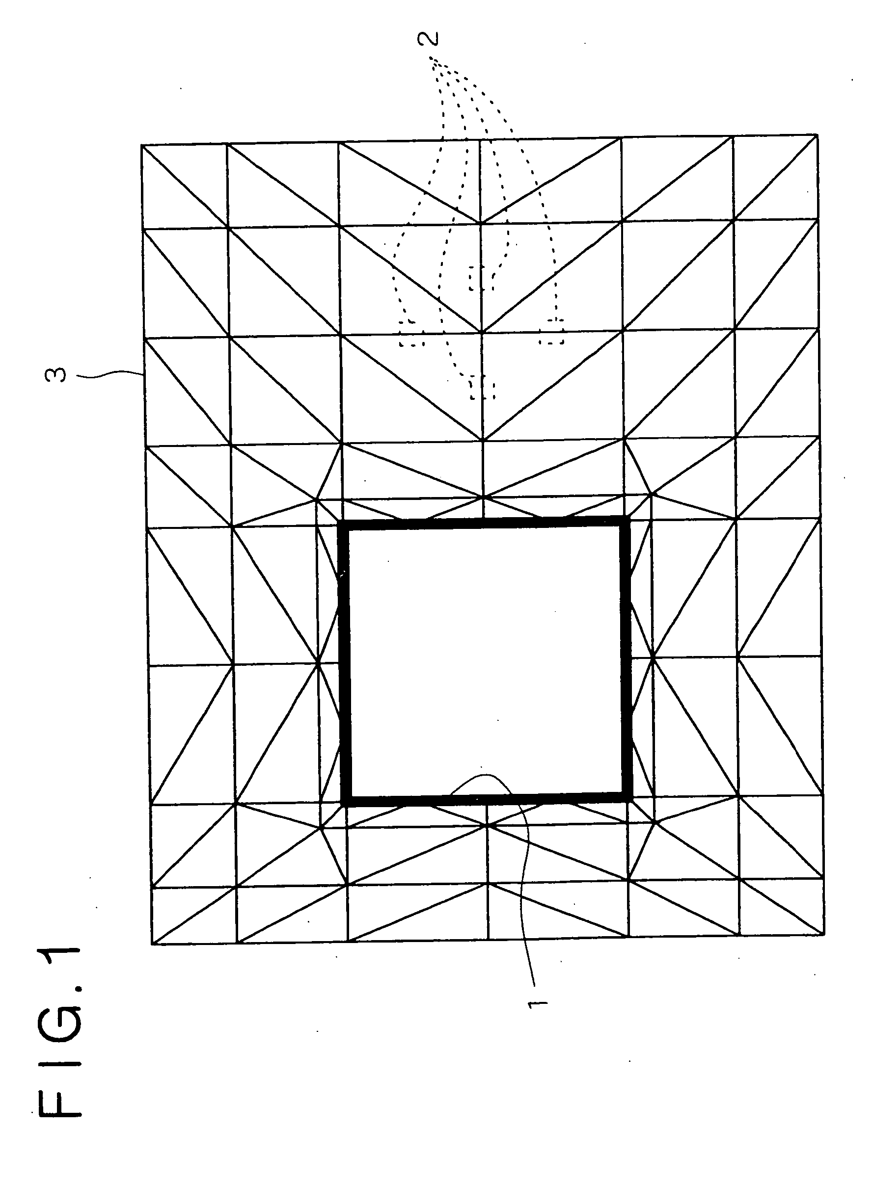
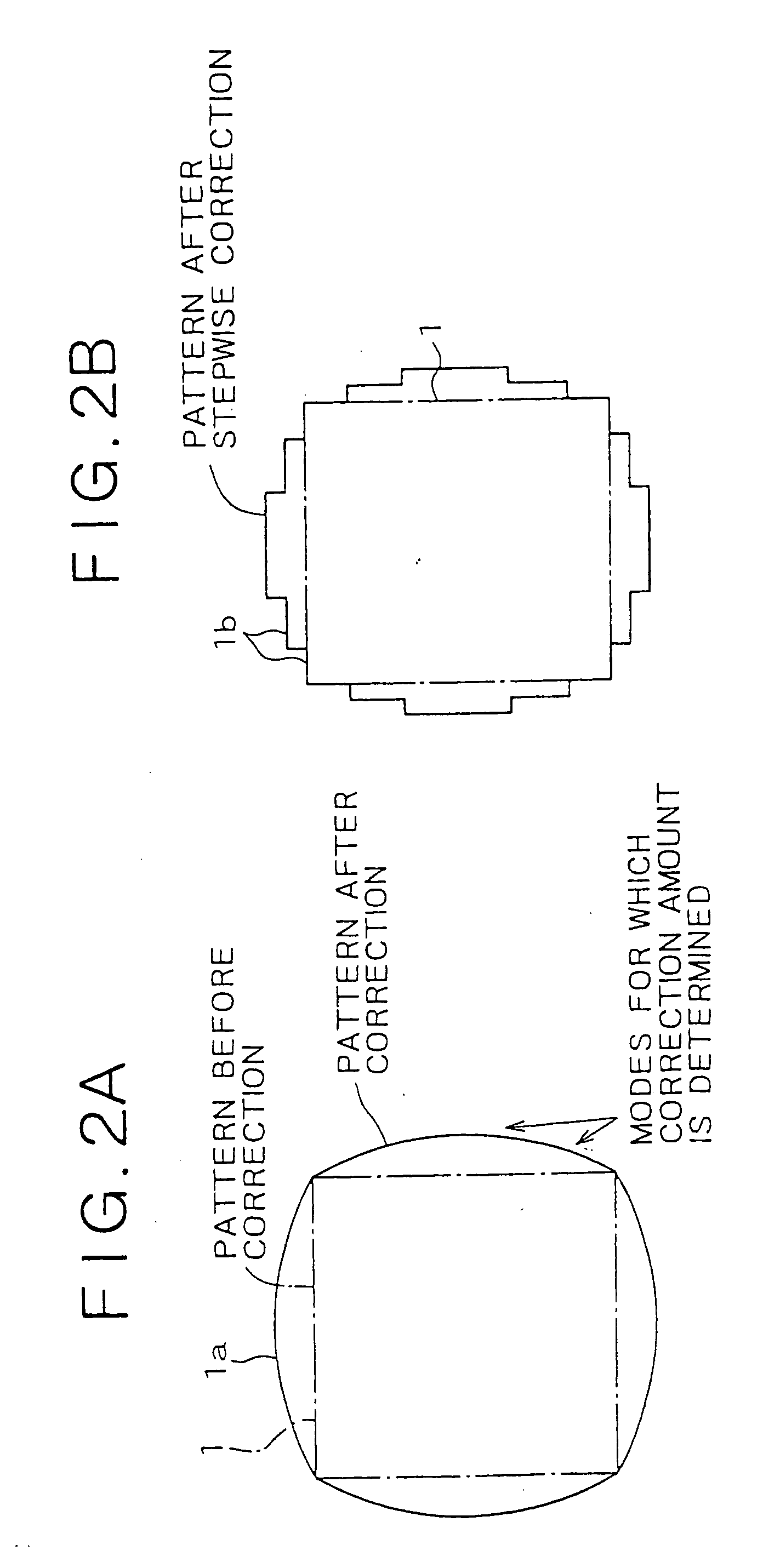
In the following, a method of producing a stencil mask to which the present invention is applied is described with reference to FIGS. 1, 2A and 2B.

Referring first to FIG. 1, a rectangular stencil mask pattern 3 having a single large stencil hole pattern 1 and four small stencil hole patterns 2 is shown. The stencil mask pattern 3 is divided into triangular elements except the large stencil hole pattern 1; and, only the single large stencil hole pattern 1 is assumed present, while the presence of the four small stencil hole patterns 2 is ignored.

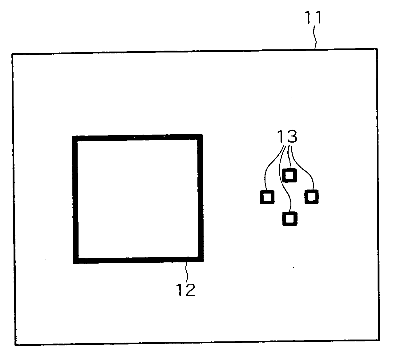
In the stencil mask pattern 3 shown, for example, the large stencil hole pattern 1 has a shape of a square having sides of 10 μm, and the small stencil hole patterns 2 have a shape of a square having sides of 100 nm. The numbers and the arrangement of the stencil hole patterns 1 and 2 are substantially the same as those of the stencil mask 11 of FIG. 3B.

Since, according to the stress analysis by the finite-element method, only a simple...


PUM

PropertyMeasurementUnit
sizeaaaaaaaaaa
plane stress analysisaaaaaaaaaa
areaaaaaaaaaaa

Abstract

A stencil mask is disclosed which can be produced by performing pattern correction in a practically applicable comparatively short period of time. When stencil mask pattern data are corrected by a stress analysis, displacement amounts are calculated for those of stencil hole patterns which have a size equal to or greater than a predetermined size. As a result, stencil mask pattern data having corrected patterns are obtained in a comparatively short period of time which can be applied industrially. By producing a stencil mask based on the patterns, a stencil mask in which a desired pattern is formed is obtained.

Description

BACKGROUND OF THE INVENTION This invention relates to a stencil mask wherein the shape of a stencil hole is corrected, a method of producing the stencil mask, a semiconductor device produced using the stencil mask and a method of producing the semiconductor device. Semiconductor devices continue to be refined more and more such that the patterning thereof with light is getting more and more difficult. Thus, lithography techniques based on an X-ray, an electron beam, an ion beam and so forth have been proposed, investigated and developed. One of the novel techniques uses a stencil-like mask formed from a plate which does not allow a used beam to transmit therethrough and having a hole of a desired pattern shape formed therein for allowing the beam to pass through, which is different from a mask structure conventionally used in light lithography and formed from a hard plate which allows a used beam to transmit therethrough and having a pattern provided thereon by a substance which ...

Claims


Application Information

Patent Timeline
Patent Type & Authority Applications(United States)
IPC IPC(8): G03F1/20G03F1/22G03F1/68G03F1/70G06F17/50H01L21/027
CPCG03F1/20
Inventor ASHIDA, ISAO
Owner ASHIDA ISAO
Learn More