Manufacturing method of organic electroluminescence display device

Inactive Publication Date: 2005-01-06
HITACHI DISPLAYS
View PDF3 Cites 6 Cited by
  • Summary
  • Abstract
  • Description
  • Claims
  • Application Information

AI Technical Summary

Benefits of technology

[0023] Further, with respect to a method which uses a bank material having a critical surface tension of not more than 30 dyne / cm and which is water-repellant and oil-repellant against ink, the method requires a bank forming process using a photolithography method, and, hence, the number of fabrication steps and the manufacturing cost are increased. Further, the use of bank material having a critical surface tension of not more than 30 dyne / cm limits the range of selection of bank materials.
[0030] Further, according to another aspect of the method of manufacture of an organic electroluminescence display device of the present invention, after forming an outer wall layer which surrounds a region where anodes are formed, non-affinity regions are formed on surfaces of the anodes by exposing the light transmitting glass substrate under a saturated vapor pressure of an organic solvent, thus adhering organic substances to the surfaces of the anodes, and affinity regions are formed by irradiating ultraviolet rays to pixel center portions, except for electrode surface peripheral portions of the anodes. Accordingly, it is possible to increase the difference between the affinity and the non-affinity for a conductive polymer material solution between the ultra-violet ray irradiated portion and the ultra-violet ray non-irradiated portion.

Problems solved by technology

However, in the technology referred to above, to form a hole injection layer and a light emitting layer having a thickness of several tens nm using ink having 0.2 to 5% of polymer concentration, it is necessary to form extremely high banks having a thickness of several μm, and, hence, there arises a drawback in that the breaking of steps of the cathodes may easily occur.
Further, although it is desirable to form black banks to enhance the contrast of the organic electroluminescence element, it is extremely difficult to form the black banks having a thickness of approximately several μm using a photolithography method in view of the optical transmissivity.
Further, with respect to a method which uses a bank material having a critical surface tension of not more than 30 dyne / cm and which is water-repellant and oil-repellant against ink, the method requires a bank forming process using a photolithography method, and, hence, the number of fabrication steps and the manufacturing cost are increased.
Further, the use of bank material having a critical surface tension of not more than 30 dyne / cm limits the range of selection of bank materials.
Still further, with respect to a bank structure which is formed by stacking a material having an affinity with the organic material and a material having a non-affinity with the organic material, the bank structure requires the formation of a bank using a photolithography method, a fluorine plasma treatment process applied to the banks for repelling liquid and the like, and, hence, the number of fabrication steps and the manufacturing cost are increased.
Further, in the typical color filter manufacturing method, the structure which makes the pixel portions on the substrate obtain an affinity to ink by irradiating energy rays to the pixel portions requires a bank forming process using a photolithography method and a process such as the irradiation of energy rays, and, hence, the number of fabrication steps and the manufacturing cost are increased.

Method used


Image

  • Manufacturing method of organic electroluminescence display device
  • Manufacturing method of organic electroluminescence display device
  • Manufacturing method of organic electroluminescence display device

Examples


Embodiment Construction

[0051] The mode for carrying out the present invention will be explained in detail in conjunction with the drawings, which show various embodiments of the invention.

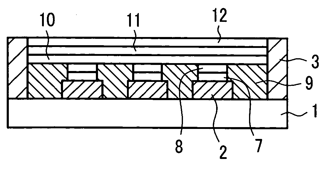
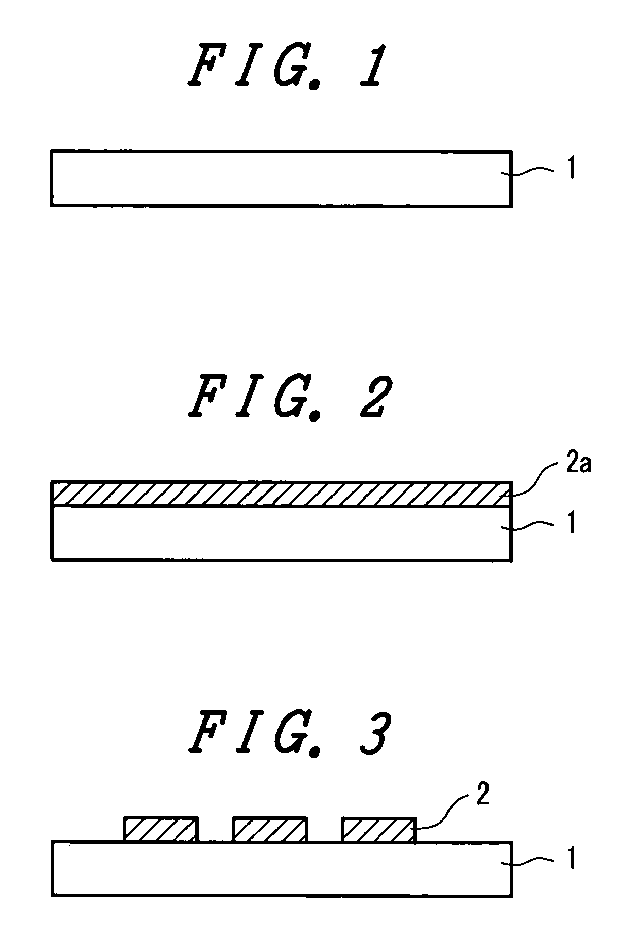
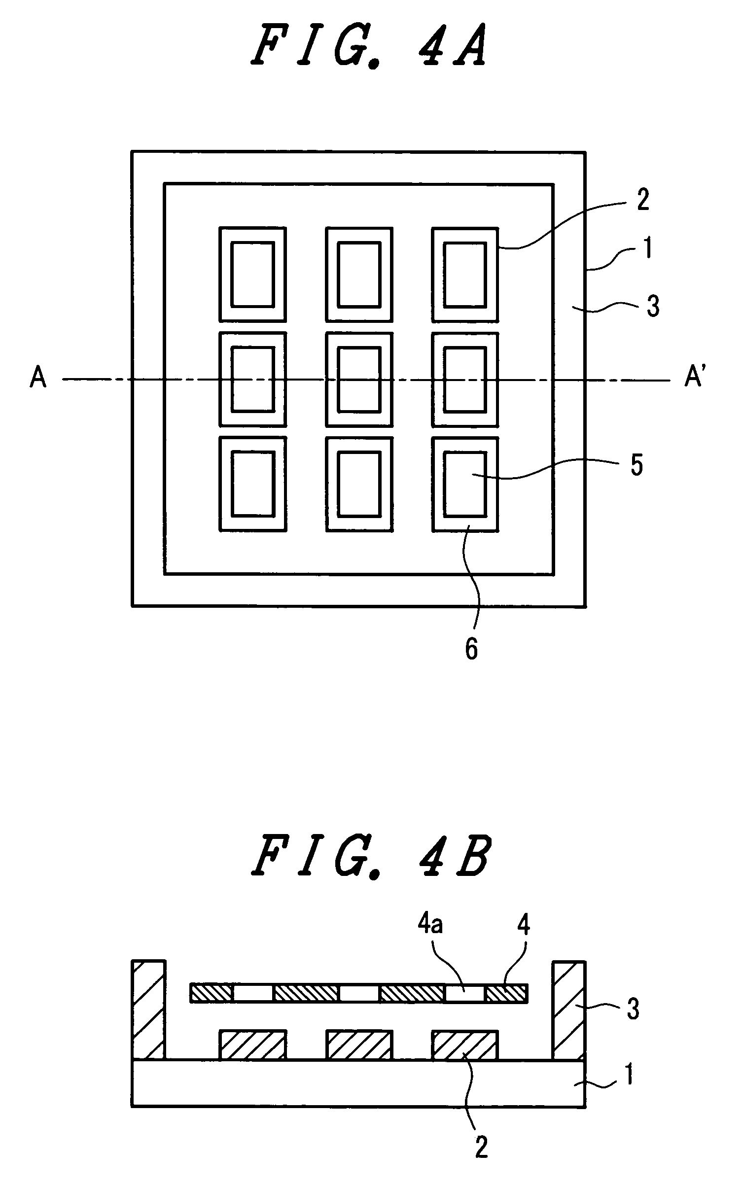
[0052]FIG. 1 to FIG. 10 are cross-sectional views, partially including plan views, of respective steps in the method of manufacture of an organic electroluminescence display device according to the present invention. First of all, on a light transmitting glass substrate 1 having a thickness of approximately 1.1 mm, as shown in FIG. 1, an ITO film 2a having a film thickness of approximately 150 nm is formed by a sputtering method, as shown in FIG. 2. Thereafter, the ITO film 2a is partially etched by a photolithography method to form a plurality of anodes 2, which constitute pixel portions and have a size of approximately 150 μm×170 μm, by patterning for every pixel, as shown in FIG. 3.

[0053] Subsequently, on the glass substrate 1 on which these anodes 2 are formed, an organic material solution (ink) containing polyimid...


PUM


Abstract

A method of manufacture of an organic electroluminescence display device includes (1) a first step of forming a non-affinity region in a surface of an anode provided in each of the pixels arranged on a glass substrate by exposing the glass substrate in a saturated vapor pressure of an organic solvent, (2) a second step of forming an affinity region in a central portion of the anode surface spaced from its edges by irradiating the central portion of the anode surface with ultraviolet light, and (3) a third step of forming polymer material layers which constitute an organic electroluminescent element in each of the pixels in the affinity region by blowing off polymer material solutions onto the affinity region of the anode in the each of the pixels. In this way, it is possible to simplify the steps in, to reduce the cost for, and to improve the productivity of the process of manufacture of the organic electroluminescence display device.

Description

[0001] The present application claims priority from Japanese application JP 2003-154715, filed on May 30, 2003, the content of which is hereby incorporated by reference into this application. BACKGROUND OF THE INVENTION [0002] The present invention relates to a method of manufacture of an organic electroluminescence display device using organic electroluminescence, and, more particularly, the invention relates to an image forming method in which a polymer light emitting material solution is held and formed at given pixel center portions while making the formation of partition walls (banks) which define the pixels unnecessary. [0003] An organic electroluminescence device, which utilizes mainly an organic material as field light emitting elements, is suitable for an application as a planar display; and, hence, an extensive development has been under way and the remarkable progress has been made in fields such as materials, element structures, fabrication techniques for light emission....

Claims


Application Information

Patent Timeline
IPC IPC(8): H01L21/00H05B33/10H01L27/32H01L51/50H01L51/52H01L51/56H05B33/14
CPCH01L27/3246H01L51/0005H01L51/56H01L51/5246H01L51/5284H01L51/5237H10K71/135H10K59/122H10K50/8426H10K50/865H10K50/844H10K71/00
Inventor YASUKAWA, AKIKOUCHINO, SHOICHIYAMADA, EMIKOHAYASHI, NOBUAKI
Owner HITACHI DISPLAYS
Why Eureka
Try Eureka