Cascaded organic electroluminescent device having connecting units with N-type and P-type organic layers

Active Publication Date: 2005-08-30
GLOBAL OLED TECH
View PDF7 Cites 179 Cited by
  • Summary
  • Abstract
  • Description
  • Claims
  • Application Information

AI Technical Summary

Benefits of technology

[0013]An advantage of the present invention is that it enables a cascaded OLED to function with improved light extraction by adjusting the physical spacing between adjacent electroluminescent zones. A further feature is that the thickness of the doped organic p-n junction structure can be adjusted to change the physical spacing between adjacent electroluminescent zones without significantly changing the driving voltage and the transparency in the emissive spectral range.
[0014]Another advantage of the present invention is that it enables a cascaded OLED to function with a doped organic p-n junction structure, thereby simplifying the fabrication steps.
[0015]Another advantag

Problems solved by technology

However, each OLED unit in their devices needs a separate power source.
These device architectures present serious fabrication difficulties.
Second, due to their thickness limitation, these electrodes cannot be used as spacers to adjust the light reflecting length in the device for improving light extraction.
Third, if an intermediate electrode is a discontinuous layer,

Method used


Image

  • Cascaded organic electroluminescent device having connecting units with N-type and P-type organic layers
  • Cascaded organic electroluminescent device having connecting units with N-type and P-type organic layers
  • Cascaded organic electroluminescent device having connecting units with N-type and P-type organic layers

Examples


Example

Example 1 (Conventional OLED—Comparative)

[0152]The preparation of a conventional non-cascaded OLED is as follows: A ˜1.1 mm thick glass substrate coated with a transparent ITO conductive layer was cleaned and dried using a commercial glass scrubber tool. The thickness of ITO is about 42 nm and the sheet resistance of the ITO is about 68 Ω / square. The ITO surface was subsequently treated with oxidative plasma to condition the surface as an anode. A layer of CFx, 1 nm thick, was deposited on the clean ITO surface as the HIL by decomposing CHF3 gas in an RF plasma treatment chamber. The substrate was then transferred into a vacuum deposition chamber for deposition of all other layers on top of the substrate. The following layers were deposited in the following sequence by sublimation from a heated boat under a vacuum of approximately 10−6 Torr:[0153](1) a HTL, 90 nm thick, consisting of NPB;[0154](2) a LEL, 20 nm thick, consisting of Alq host doped with 1.0 vol. % C545T;[0155](3) an ET...

Example

Example 2 (Inventive)

[0160]The preparation of a cascaded OLED with two EL units is as follows: A ˜1.1 mm thick glass substrate coated with a transparent ITO conductive layer was cleaned and dried using a commercial glass scrubber tool. The thickness of ITO is about 42 nm and the sheet resistance of the ITO is about 68 Ω / square. The ITO surface was subsequently treated with oxidative plasma to condition the surface as an anode. A layer of CFx, 1 nm thick, was deposited on the clean ITO surface as the HIL by decomposing CHF3 gas in an RF plasma treatment chamber. The substrate was then transferred into a vacuum deposition chamber for deposition of all other layers on top of the substrate. The following layers were deposited in the following sequence by sublimation from a heated boat under a vacuum of approximately 10−6 Torr:[0161](1) a first HTL, 60 nm thick, consisting of NPB as a spacer between transparent anode and the first EL unit;[0162](2) a HTL, 30 nm thick, consisting of NPB;[...

Example

Example 3 (Inventive)

[0178]A cascaded OLED with three EL units was fabricated as the same as Example 2 except that after step (9) in Example 2, steps (5) to (9) are repeated once to add one more connecting unit and one more EL unit, followed by steps (10) and (11).

[0179]After the deposition of these layers, the device was transferred from the deposition chamber into a dry box for encapsulation. The completed device structure is denoted as

ITO / CFx / NPB(60) / EL / CU / EL / CU / EL / Alq(30) / Mg:Ag.

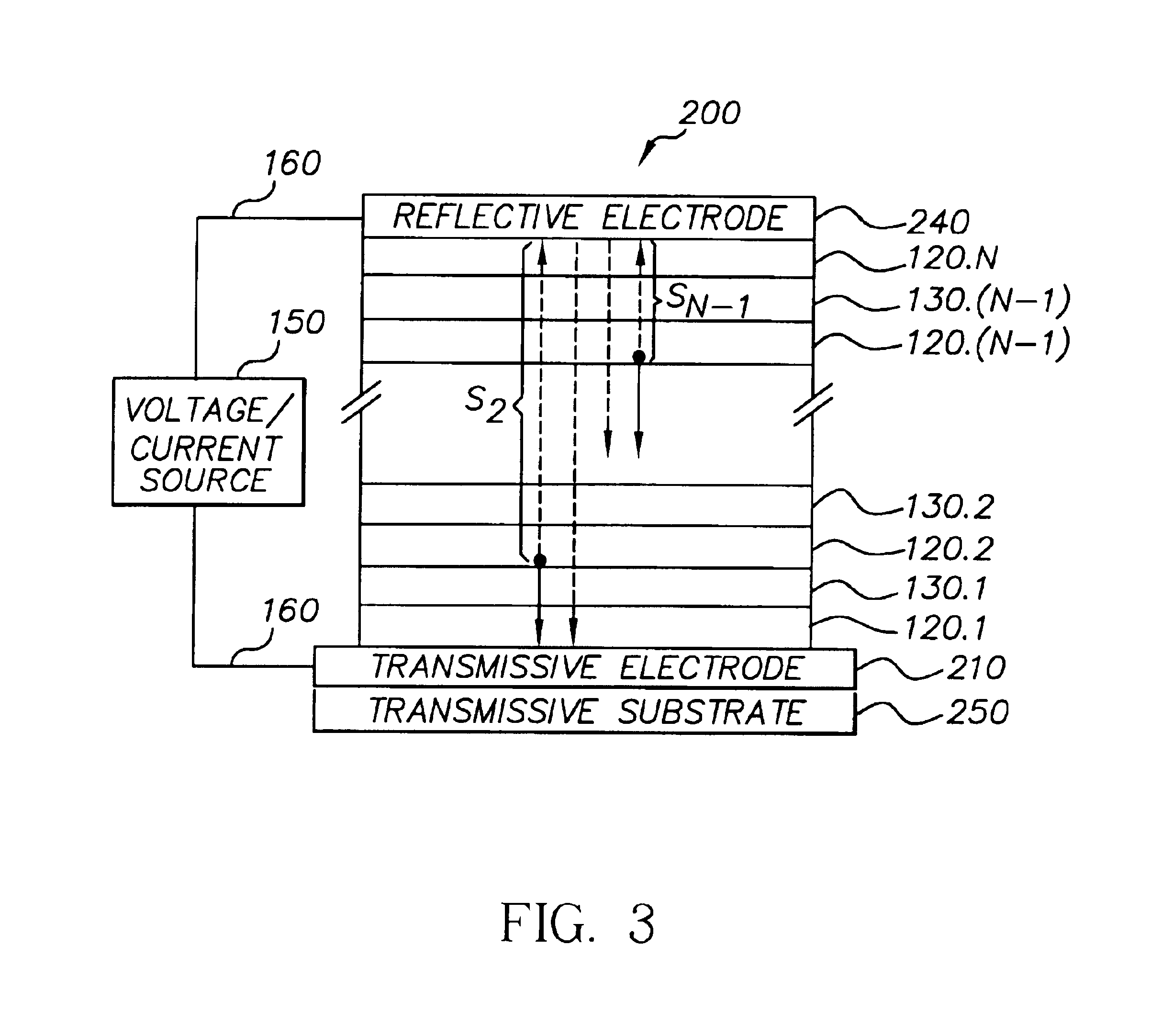
[0180]In this cascaded OLED, the same as )in Example 2, the connecting unit has a resistivity higher than 10 Ω-cm and an optical transmission higher than 90%. The peak emission wavelength λ from each LEL is 524 nm. S3=S3,O=95 nm, S2=1.01×S2,O=362 nm, and S1=1.02×S1,O=1.02×619=629 nm. The optical distances from each emitting central plane to the reflective Mg:Ag cathode have been optimized. Moreover, the physical spacing between each of the emitting central planes is 150 nm, which is corresponding to an op...


PUM


Abstract

A cascaded organic electroluminescent device includes an anode and a cathode. The device also includes a plurality of organic electroluminescent units disposed between the anode and the cathode, wherein the organic electroluminescent units comprise at least a hole-transporting layer, an electron-transporting layer, and an electroluminescent zone formed between the hole-transporting layer and the electron-transporting layer wherein the physical spacing between adjacent electroluminescent zones is more than 90 nm; and a connecting unit disposed between each adjacent organic electroluminescent unit, wherein the connecting unit comprises, in sequence, an n-type doped organic layer and a p-type doped organic layer forming a transparent p-n junction structure wherein the resistivity of each of the doped layers is higher than 10 Ω-cm.

Description

CROSS-REFERENCE TO RELATED APPLICATION[0001]Reference is made to commonly assigned U.S. patent application Ser. No. 10 / 077,270 filed Feb. 15, 2002 by Liang-Sheng L. Liao et al., entitled “Providing an Organic Electroluminescent Device Having Stacked Electroluminescent Units”, the disclosure of which is herein incorporated by reference.FIELD OF INVENTION[0002]The present invention relates to providing a plurality of organic electroluminescent (EL) units to form a cascaded organic electroluminescent device.BACKGROUND OF THE INVENTION[0003]Organic electroluminescent (EL) devices or organic light-emitting devices (OLEDs) are electronic devices that emit light in response to an applied potential. The structure of an OLED comprises, in sequence, an anode, an organic EL medium, and a cathode. The organic EL medium disposed between the anode and the cathode is commonly comprised of an organic hole-transporting layer (HTL) and an organic electron-transporting layer (ETL). Holes and electrons...

Claims


Application Information

Patent Timeline
IPC IPC(8): H01L27/32H01L27/28H05B33/12H01L51/50H01L51/52H05B33/18
CPCH01L51/5278H10K50/19A44C5/2076A44C15/005
Inventor LIAO, LIANG-SHENGKLUBEK, KEVIN P.COMFORT, DUSTIN L.TANG, CHING W.
Owner GLOBAL OLED TECH
Why Eureka
Try Eureka