Process for preparing a stabilized ideal oxygen precipitating silicon wafer

Active Publication Date: 2005-01-13
GLOBALWAFERS CO LTD
View PDF28 Cites 15 Cited by
  • Summary
  • Abstract
  • Description
  • Claims
  • Application Information

AI Technical Summary

Benefits of technology

Briefly therefore, the present invention is directed to a process for the preparation of a single crystal silicon wafer having a controlled oxygen precipitation behavior. The process comprises selecting a wafer sliced from a single crystal silicon ingot grown by the Czochralski method comprising a front surface, a back surface, a central plane between the front and back surfaces, a front surface layer which comprises the region of the wafer between the front surface and a distance D measured from the front surface and toward the central plane, and a bulk layer which comprises the region of the wafer between the central plane and the front surface layer. The selected wafer is heated to an annealing temperature TA to form crystal lattice vacancies in the front surface and bulk layers of the wafer. The heated wafer is cooled from TA to an upper nucleation temperature TU at a rate R to form a vacancy concentration profile in the wafer wherein the peak density of vacancies is in the bulk layer with the concentration generally decreasing from the location of the peak density in the direction of the front surface of the wafer. The vacancy profiled wafer is maintained within a nucleation temperature range that is bounded by TU and a lower nucleation temperature TL for a nucleation duration tn to form oxygen precipitate nucleation centers in the bulk layer that are incapable of being dissolved at temperatures below about 1150° C. and a region free of oxygen precipitate nucleation centers in the surface layer. The concentration of oxygen precipitate nucleation centers in the bulk layer is dependent upon the concentration of vacancies.
The present invention is also directed to a process for the preparation of a single crystal silicon wafer having a controlled oxygen precipitation behavior. The process comprises selecting a wafer sliced from a single crystal silicon ingot grown by the Czochralski method comprising a front surface, a back surface, a central plane between the front and back surfaces, a front surface layer which comprises the region of the wafer between the front surface and a distance D measured from the front surface and toward the central plane, and a bulk layer which comprises the region of the wafer between the central plane and the front surface layer. The wafer is heated to an annealing temperature TA that is at least about 1300° C. to form crystal lattice vacancies in the front surface and bulk layers. The heated wafer is cooled from TA to an upper nucleation temperature TU that is between about 1020 and about 1090° C. at a rate R that is between about 40 and 50° C./sec to form a vacancy concentration profile in the wafer wherein the peak density of vacancies is in the bulk layer with the concentration generally decreasing from the location of the peak density in the direction of the front surface of the wafer. The vacancy concentration profiled wafer is maintained within a nucleation temperature range that is bounded by TU and a lower nucleation temperature TL that is between about 1000 and about 1080° C. wherein the difference between TU and TL is no greater than about 20° C. and generally decreases as TU and TL increase. The wafer is maintained with the nucleation temperature range for a nucleation duration tn that is between about 10 and about 30 seconds to form oxygen precipitate nucleation centers in the bulk layer that are incapable of being dissolved at temperatures below about 1150° C. and a region free of oxygen precipitate nucleation centers in the surface layer, with the concentration of oxygen precipitate nucleation centers in the bulk layer being dependent upon the concentration of vacancies.
Additionally, the present invention is directed to a process for the p

Problems solved by technology

As molten silicon is contained in a quartz crucible, it is contaminated with various impurities, among which is mainly oxygen.
Depending upon their location in the wafer, the precipitates can be harmful or beneficial.
Oxygen precipitates located in the active device region of the wafer can impair the operation of the device.
Although some of these processes retain enough of the high temperature process steps to produce a denuded zone

Method used


Image

  • Process for preparing a stabilized ideal oxygen precipitating silicon wafer
  • Process for preparing a stabilized ideal oxygen precipitating silicon wafer
  • Process for preparing a stabilized ideal oxygen precipitating silicon wafer

Examples


Embodiment Construction

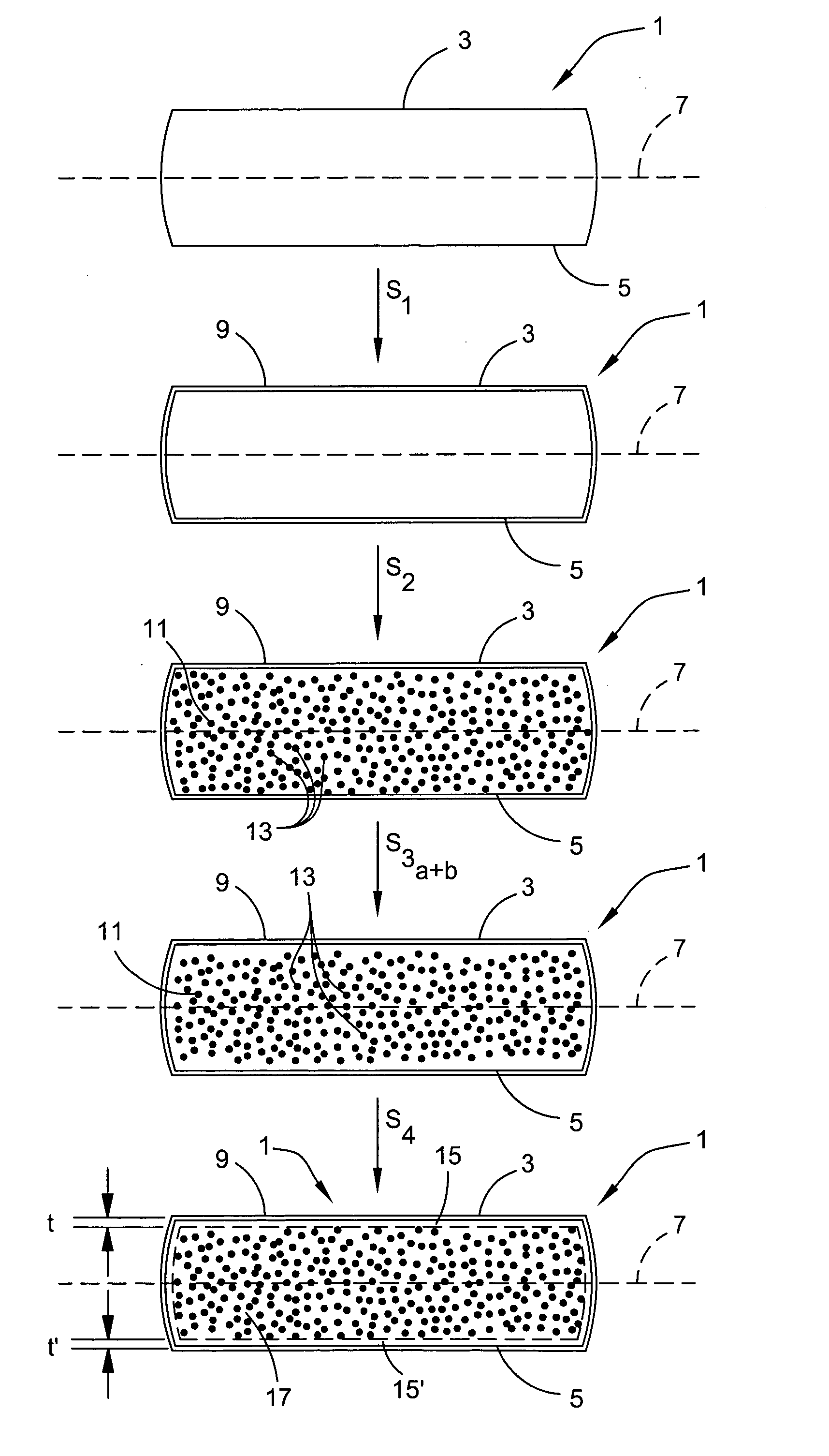
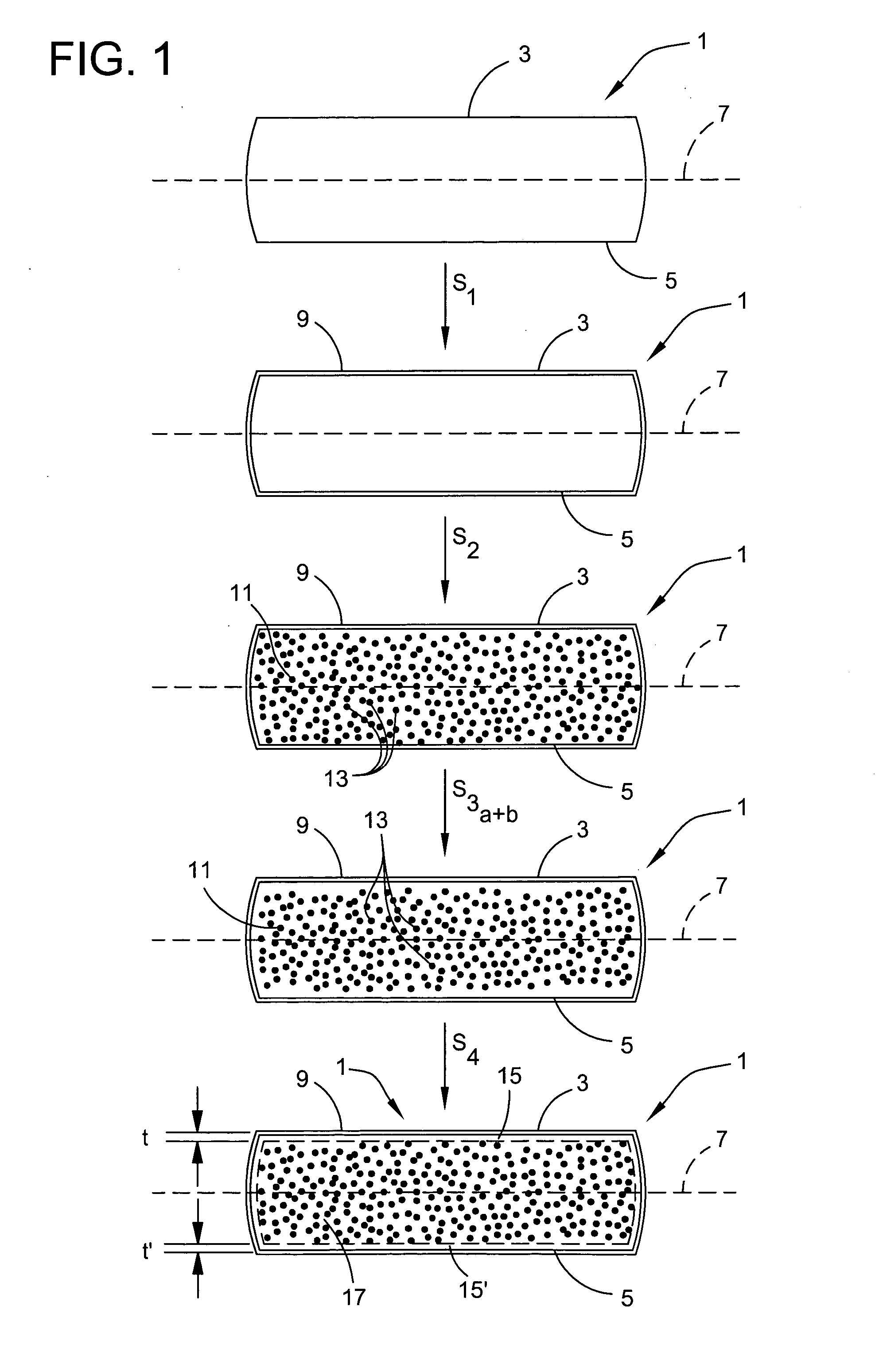
In accordance with the present invention, an ideal precipitating wafer has been discovered which, during essentially any electronic device manufacturing process, will form a denuded zone, or precipitate-free region, of sufficient depth and a wafer bulk containing a sufficient density of oxygen precipitates for intrinsic gettering purposes. Advantageously, this ideal precipitating wafer may be prepared in a matter of minutes using tools which are in common use in the semiconductor silicon manufacturing industry. This process creates a “template” in the silicon which determines or “prints” the manner in which oxygen will ultimately precipitate. In accordance with the present invention, the process for forming this template is controlled so that oxygen precipitate nucleation centers formed in the wafer bulk are stabilized such that they may survive a subsequent rapid thermal heat treatment (e.g., epitaxial deposition and / or oxygen implantation) without an intervening thermal stabiliza...


PUM


Abstract

The present invention is directed to a single crystal Czochralski-type silicon wafer, and a process for the preparation thereof, which has a non-uniform distribution of stabilized oxygen precipitate nucleation centers therein. Specifically, the peak concentration is located in the wafer bulk and a precipitate-free zone extends inward from a surface.

Description

BACKGROUND OF THE INVENTION The present invention generally relates to the preparation of semiconductor material substrates, especially silicon wafers, which are used in the manufacture of electronic components. More particularly, the present invention is directed to a process for treating a silicon wafer to form an ideal, non-uniform depth distribution of stabilized oxygen precipitates, i.e., the size of the oxygen precipitates is sufficient to withstand being rapidly heated to temperatures not in excess of 1150° C. Single crystal silicon, which is the starting material for most processes for the fabrication of semiconductor electronic components, is commonly prepared with the so-called Czochralski process wherein a single seed crystal is immersed into molten silicon and then grown by slow extraction. As molten silicon is contained in a quartz crucible, it is contaminated with various impurities, among which is mainly oxygen. At the temperature of the silicon molten mass, oxygen ...

Claims


Application Information

Patent Timeline
IPC IPC(8): C30B33/00
CPCC30B33/00C30B29/06H01L21/20
Inventor FALSTER, ROBERT J.VORONKOV, VLADIMIR V.
Owner GLOBALWAFERS CO LTD
Why Eureka
Try Eureka